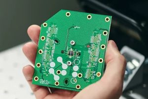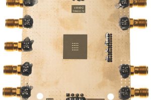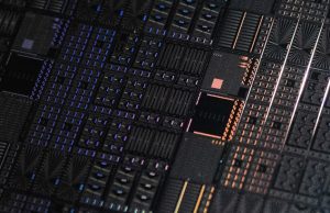
The devices had an average charge noise of 0.6µeV/√Hz at 1Hz.
“In view of noise performance, the values obtained are the lowest charge noise values achieved on a 300mm fab-compatible platform,” according to the Belgian research lab. “By demonstrating those values, repeatedly and reproducibly this work makes large-scale quantum computers based on Si quantum dots a realistic possibility.”
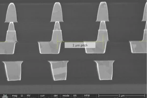
The 300mm CMOS production line was modified for silicon MOS (metal-oxide-semiconductor) qubit integration, with the gate-stack changed to allow quantum dots to be created at the silicon-SiO2 interface.
“Si quantum dot spin qubits are promising building blocks to realise large-scale quantum computers for two main reasons,” explained Imec:
First: Si spin qubits with long quantum coherence times, and high-fidelity quantum gate operations, have been repeatedly demonstrated in lab environments and are a technology with realistic prospects.
Second: the underlying technology is compatible with CMOS manufacturing and offers the possibility of wafer-scale uniformity and yield, with the required back-end-of-line interconnection of the Si quantum dot structures that are needed for truly large scale quantum chips, with millions or even billions of qubits operating in synchrony.
Imec is pursuing several types of silicon quantum dot spin qubits. In the demonstration, they were defined by MOS quantum dot structures that resemble transistors, which can trap a single spin of an electron or hole.
A source of performance-sapping noise is residual charges trapped near or inside the quantum dot, so defects need to be minimised.
Lab-based techniques such gentle lift-off can reduce process damage, while production techniques such as subtractive etch and lithography-based patterning can easily degrade device quality, particularly at the Si-SiO2 interface near the quantum dot qubits – leading to lab-made qubits typically our-performing those made on production equipment.
“We demonstrated charge noise levels that, depending on the source, are between half an order of magnitude to one order of magnitude lower, when compared to current state-of-the-art fab-based silicon quantum dot structures and achieved remarkably uniform quantum dot operation,” said Imec quantum computing director Kristiaan De Greve. “Our results confirm that 300mm silicon MOS is a compelling material platform for quantum dot spin qubits, and highlight the maturity of industrial fabrication techniques for qubit development.”
The statistical analysis methods used to characterise the charge noise revealed fundamental insights into the origin.
“Knowing the source of the charge noise will give us directions to further optimise the structures,” said De Greve, adding that quantum computers “with current understanding, will require millions of physical qubits.”
The work is published as ‘Low charge noise quantum dots with industrial CMOS manufacturing‘ in Nature’s npj Quantum Information – which can be read in full without payment.
 Electronics Weekly Electronics Design & Components Tech News
