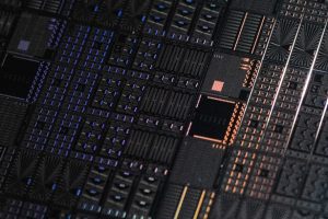
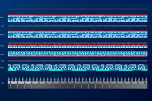
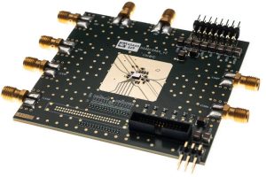
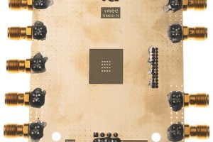
Imec has used 300mm wafers to demonstrate silicon-based quantum dot spin qubit processing. The devices had an average charge noise of 0.6µeV/√Hz at 1Hz. “In view of noise performance, the values obtained are the lowest charge noise values achieved on a 300mm fab-compatible platform,” according to the Belgian research lab. “By demonstrating those values, repeatedly and reproducibly this work makes ...
Tag Archives: IMEC
CMOS 2.0
Julien Ryckaert at imec suggests a new approach to heterogeneous integration – instead of heterogeneous packaging, use monolithic heterogeneous on-chip integration. Ryckaert calls the approach ‘CMOS 2.0’. “For several decades, the advancement of monolithic systems-on-chip (SoCs) for high-performance computing (HPC) – such as CPUs and GPUs – hinged on the success of CMOS scaling,” says Ryckaert, “CMOS offered SoC developers ...
What caught your eye this week? (Efabless, Imec 2nm, 402Tbit/s, ESA)
We're talking democratising chip design, training for Imec's 2nm PDK, 402Tbit/s down standard optical fibre, and ESA's Zero Debris charter...
Europe to get 10nm and 7nm FD-SOI pilot line
A European pilot line for digital, analogue and RF ICs on 10nm and 7nm FD-SOI was announced today at French research lab CEA-Leti in Grenoble. Called Fames Pilot Line, it will create manufacturing processes for OxRAM, FeRAM, MRAM and FeFETs embedded non-volatile memories; RF switches, filters and capacitors; integrated inductors for dc-dc converters; and both heterogeneous and sequential 3D integration. ...
VLSI Symposium: RF ADCs cover 5GHz
At the IEEE VLSI Symposium this week, Imec revealed two ADCs for 5GHz ‘beyond 5G’ communication, one for base stations and one for phones. The base station ADC operates over bands up to 5GHz. It is a 10Gsample/s cmos hierarchical time-interleaved ADC that delivers 9 ENOB (effective number of bits) at low frequencies and 8.2 ENOB at Nyquist. SFDR (spurious-free ...
Graphene update – the wafers have landed
As the first phase of the Graphene Flagship’s 2D Experimental Pilot Line (2D-EPL) project draws to a close, some of the partners provided an update on its progress to establish a European ecosystem and move graphene wafers out of the laboratory environment and into full wafer production. One of the partners, Graphenea, manufactures and commercialises different graphene materials. Its scientific ...
56Gbit/s zero-IF D-band beam-forming transmitter for 120-145GHz comms
Imec unveiled a CMOS 56Gbit/s zero-IF D-band beam-forming transmitter at the IEEE RFIC Symposium in Washington. “It is a key component of a 4-way beamforming transceiver chip currently being developed by imec’s researchers,” according to the Belgian research lab. “With this technology, they aim to support the deployment of short-range wireless services at frequencies above 100GHz.” It sees Gbit/s communication ...
Imec develops die-to-wafer bond process with 2µm pad pitch
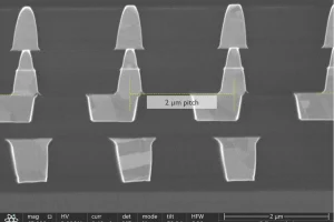
Imec has developed a Cu-to-Cu and SiCN-to-SiCN die-to-wafer bonding process resulting in a Cu bond pad pitch of only 2µm at <350nm die-to-wafer overlay error, achieving good electrical yield. Such fine-grained die-to-wafer interconnects pave the way to logic/memory-on-logic and memory-on-memory applications. On the longer term, die-to-wafer bonding will enable also die- and wafer-level optical interconnects – for which imec demonstrated ...
Most Read Articles – Quantum, 2nm process, Semiconductor Institute
For those written this week, the most popular stories involve the quantum market, integrating RFID tyre tags into tyres, Imec building a pilot line for processes beyond 2nm, and the UK government setting up a Semiconductor Institute...
Chip analyses human white blood cells
Imec has teamed up with Sarcura, an Austrian start-up, to build an white blood cell analyser-on-a-chip using integrated photonics. Resolution is sufficient to discriminate between lymphocytes and monocytes, “rivaling the performance of commercial cytometers”, said Imec scientific director Niels Verellen. It is a flow cytometer and is based on the scattering of a laser beam though a sample. The intensities ...
 Electronics Weekly Electronics Design & Components Tech News
