For some engineers the term JTAG means a device programming port. For others it exists to plug in a microprocessor emulator or debugger. Originally it was devised for neither of these applications. The acronym JTAG stands for the Joint Test Action Group and its initial aims were to provide an alternative system approach for circuit board assembly testing, that is, detecting and diagnosing assembly errors such as solder shorts, lifted pins and missing/badly placed devices.
The Group part refers to a small number of test professionals who met over a number of years in the late 1980s to devise a scheme to embed test circuitry into digital devices with the aim of assisting in the structural test of the printed circuit board assembly PCBA(s). Similar schemes had been developed unilaterally by device manufacturers (for example, IBM’s Level Sensitive Scan Design technique), but at that point there was no standard with which all vendors could comply that allowed interoperability.
By 1990 the system, also known as boundary scan, was an official IEEE standard (number 1149.1).
Alternative uses
Soon after its formal introduction, the alternative uses for JTAG were developed, for example, as a [firmware] debugger port and as a device programming port. This commandeering of the JTAG port for debugging can be attributed to silicon chip companies such as TI and Arm, which realised that the compact four-wire interface and a state machine could be used to access internal debug registers as well as the IEEE Std 1149.1 (boundary scan) test registers defined by the JTAG committee.
At this point it might have been useful to define a new name for this class of activity. (Along with the original JTAG for board test, there was also JTAG for debug, although the latter is not covered by the IEEE standard.) To confuse matters further, Intel introduced a range of programmable logic devices in 1993 that were the among the first to use the JTAG port for directly accessing configuration/programming registers for the logic fabric, resulting in another use: JTAG for programming.
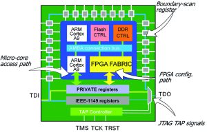
Figure 1: Graphic showing JTAG aspects of a modern FPGA/SoC such as AMD
Xilinx Zynq devices
Thus, within three years of its formal existence, the JTAG committee’s test port spawned two other applications: Risc/DSP processor debug and device on-board programming. Today, 30 years later, the market includes devices that feature all three aspects of JTAG. AMD’s Xilinx Zynq SoCs, for example, contain a processor section with dual Arm A9 cores and a programmable section configured by JTAG as well as a regular IEEE Std 1149.1 boundary-scan sub-system (see Figure 1).
Evolving tool-sets
At the inception of the standard in 1990 JTAG tools were obviously rather basic and covered only the PCBA ‘test’ aspect. Some automatic test program generators existed for creating pin-pin interconnect tests, but they still required a significant input of design knowledge from the users in order to set ‘safe’ test conditions on the target design. Memories and logic device (cluster) tests followed in the mid-1990s when tools such as Memory Test Program Generator used rudimentary modelling files to assist the program generators. Next, came the support for in-system programming of CPLDs (Altera, Cypress, Lattice, Xilinx etc) and then parallel flash memories. It was at this stage in the development of JTAG technology that PCB assembly manufacturers could use a common platform for structural testing and programming of boards prior to the final functional testing stage.
By the end of the 1990s JTAG/boundary-scan testing and programming was a well-established technique, used widely for early process fault detection on complex, high-value designs, so much so that some factories were able to abandon conventional structural testers (in-circuit testers) in favour of JTAG/boundary-scan. Others, meanwhile, looked for solutions that allowed them to augment their current testers with JTAG – often through third-party ‘bolt-on kits’.
Throughout the 2000s JTAG/boundary-scan tools were further refined. Ease of use reached new levels through the introduction of extensive device modelling and support for new JTAG methods such as IEEE 1149.6 (boundary-scan testing of high-speed LVDS connections) was introduced. However, throughout this time there were still few indications that the ‘JTAG for embedded debug’ and embedded test in general would become a more mainstream requirement in the factory.
Core assets
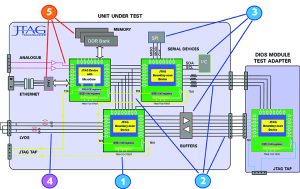
Figure 2: Summary/examples of JTAG-powered board test options on a modern digital or mixed-signal design.
Scan path infrastructure
Boundary-scan device interconnections including external test module
Boundary-scan cluster testing and programming [of non-JTAG devices]JTAG (IEEE Std.1149.6) AC-EXTEST testing of ac-coupled LVDS signals via loop-back
Testing using JTAG CoreCommander – controls device embedded peripherals to test DRR at-speed, plus ADC inputs and Ethernet PHY
Embedded memory programming using JTAG CoreCommander
By the start of the last decade, the ability to test boards using all the facets of JTAG (debug as well as test and programming) was recognised as test engineers discovered that using capabilities such as embedded processor core emulation would allow faster and potentially more thorough testing of peripherals such as complex double data rate-type memories. Furthermore, core access provides the ability to communicate with device embedded features such as ADCs and DACs, finally realising the highly desirable aspect of JTAG-powered analogue testing. Products such as CoreCommander by JTAGLive offer these capabilities and can also allow FPGAs to be configured with board test-specific IP (sometimes referred to as embedded instruments) triggered using the same test equipment as conventional boundary-scan. Dual JTAG systems offer a host of testing possibilities due to synchronisation of these assets, especially when controlled by a powerful open-source scripting language such as Python (see Figure 2).
JTAG roadmap
Technology rarely stands still and since testing has to keep pace with the products being built, JTAG has also been updated. Major updates to the base standard 1149.1 came in 2013 with a sizable addendum to the original work. Another update is due this year. Around 2014, another group that was working on an on-chip access infrastructure for embedded instruments had work ratified as IEEE 1687. This was primarily devised to improve board-level testability through the greater use of embedded test cores (BIST IP) accessed via an extended standardised infrastructure. A system level JTAG interface (SJTAG) now has a working group designation and discussions on how best to implement a standardised test method across multi-board system continue under the IEEE Std P2654 banner.
Growth opportunities
The JTAG committee’s boundary-scan test access port to aid in fault-finding on surface-mounted PCBAs has grown, with increased value to both design and test engineers. While designers can enjoy cheap and easy access to the debug registers of a microprocessor, test and production engineers can get a low-cost versatile on-board device programmer coupled to the structural tester right at the point of assembly.
There is one caveat, however. Not all standards make the cut. For example, the analogue variant (1149.4) has withered on the vine. Time will tell if the new developments will gain sufficient traction and the critical support from the semiconductor houses to make them as ubiquitous as the original format.
 Electronics Weekly Electronics Design & Components Tech News

