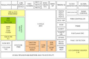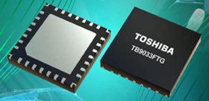
Not a lot more has been revealed about the function of the IC, called TB9033FTG, except that it has 16 GPIO pins, six of which can be inputs for a 10bit ADC, and four of which can become PWM outputs with 8bit resolution.
There is also a 4×4 switch matrix mode and fault detection for over-temperature, over-voltage and low-voltage.
On-board non-volatile memory will be included to store the configuration, and some conditions that precede an abnormality can be detected, and a report sent to the commander node on the network – the TB9033FTG can only work in ‘responder’ mode.
Toshiba’s earlier TB9032FNG, Rohm’s BD41000FJ-C (updated to BD41003FJ-C) and Infineon’s S6BT112A are 8pin CXPI bus transceivers with a Tx/Rx serial interface for a host microcontroller, so Toshiba’s statement above suggests some microcontroller-style peripherals have been co-opted into the forthcoming TB9033FTG alongside control logic – Electronics Weekly has asked for more information.
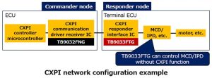 The older three (or four) have a pin/pad that allows them to be switched between ‘commander’ and ‘responder’ operation on the CXPI bus (Toshiba example left).
Some physical and electrical information has been released: operation over -40 to 125°C and 6 to 18V, with protection to +40V on some pins, and possibly -27V on the CXPI bus pad. Consumption drops to 10μA in sleep mode.
The package is a 6 x 6mm 28pad VQFN, and the IC will conform to AEC-Q100.
CXPI is a one-wire-plus-return multi-drop bus, intended to compete with LIN (local interconnect network).
“Compared to the LIN protocol, the high-speed response of the CXPI responder interface device makes it suitable for applications including steering wheel switches, meter cluster switches, light switches, and door locks and mirrors,” said Toshiba.
It is a CSMA/CR (carrier sense multiple access / collision resolution) bus that can shift data at up to 20kbit/s. ISO 20794 is its international standard.
Mass production is scheduled for December 2025.
 Electronics Weekly Electronics Design & Components Tech News
