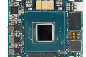
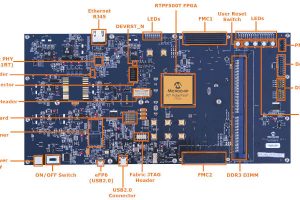
MachXO5T-NX, as they are called, are suited to “a set of control function designs for enterprise networking, machine vision and industrial IoT”, it said.
 They are built using the company’s FDSoI process (image right), which can dramatically reduce soft errors from radiation compared with bulk CMOS as there is less volume of semiconductor (orange) with access to the transistors in whicg spurious carries can be generated,
Up to 7.2Mbit of memory is included, up to 55Mbit of user flash and up to 96k logic cells (see table below).
There are up to 291 general purpose IOs “that support early IO configuration and provide added features such as 1.25Gbit/s SGMII, default pull-down, hot-socketing and programmable slew rate”, said Lattice.
Multiple IO voltages are supported (1, 1.2, 1.5, 1.8, 2.5 and 3.3V) and there are LVDS and MIPI interfaces.
PCIe and LPDDR4 interfacing feature on the larger two (53k and 96k cell) of the three announced devices.
For intellectual property protection, there is multi-boot with bit-stream encryption (AES256) and authentication (ECC256).
Packaging is 17 x 17mm with 0.8mm pitch, and there is a 14 x 14mm option for the smaller (25k cell) version.
| MachXO5-NX | MachXO5T-NX | ||
|---|---|---|---|
| Device | LFMXO5-25 | LFMXO5-55T | LFMXO5-100T |
| Logic cells | 25k | 53k | 96k |
| embedded memory blocks | 80 (x18kbit) | 166 | 208 |
| Embedded memory | 1440kbit | 2988 | 3744 |
| Distributed ram | 184kbit | 320 | 639 |
| Large memory blocks | 1 | 5 | 7 |
| Large memory bits | 512kbit | 2560 | 3584 |
| 18×18 multipliers | 20 | 146 | 156 |
| ADC blocks | 2 | 2 | 2 |
| 450MHz oscillator | 1 | 1 | 1 |
| 128kHz oscillator | 1 | 1 | 1 |
| PCIe Gen2 hard IP | 0 | 1 | 1 |
| GPLL | 2 | 4 | 4 |
| User flash (without initialisation) | 15Mbit | 79 | 79 |
Lattice sources vary on some of the numbers used in the above article and table (fact checking is under way), so check them for yourself if they are important to you.
 Electronics Weekly Electronics Design & Components Tech News


