A European pilot line for digital, analogue and RF ICs on 10nm and 7nm FD-SOI was announced today at French research lab CEA-Leti in Grenoble. Called Fames Pilot Line, it will create manufacturing processes for OxRAM, FeRAM, MRAM and FeFETs embedded non-volatile memories; RF switches, filters and capacitors; integrated inductors for dc-dc converters; and both heterogeneous and sequential 3D integration. ...
Tag Archives: FD-SOI
FD-SoI FPGAs get PCIe and LPDDR4 interfacing
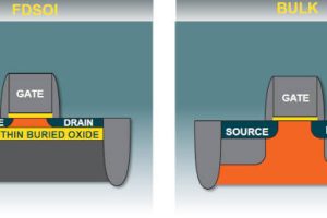
Lattice Semiconductor is aiming at system control with a family of FPGAs that includes PCIe Gen 2 interfacing and embedded security. MachXO5T-NX, as they are called, are suited to “a set of control function designs for enterprise networking, machine vision and industrial IoT”, it said. They are built using the company’s FDSoI process (image right), which can dramatically reduce soft ...
Weebit Nano tapes out demo chip
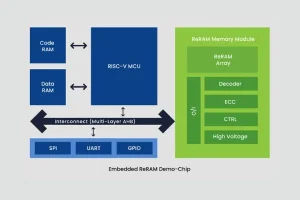
Weebit Nano has taped out a demonstration chip integrating its embedded ReRAM module on a 22nm FD-SOI process technology. This is the first tape-out of Weebit ReRAM in 22nm, one of the industry’s most common process nodes, and a geometry where embedded flash is not viable. Weebit worked with its development partners CEA-Leti and CEA-List to successfully scale its ReRAM ...
Lattice picks FD-SOI and redesigns FPGAs for embedded vision and edge AI
Lattice has switched to 28nm FD-SOI (fully-depleted silicon-on-insulator) technology for a range of sram-based FPGAs intended for embedded vision and artificial intelligence processing in industrial, automotive and consumer systems. Although they are ram-based, and therefore need to boot from adjacent memory, the firm has found a way to get chip outputs enabled, set and stable within 3ms of power-up – allowing ...
GloFo and eVaderis develop MRAM for MCU on 22nm FD-SOI
Globalfoundries and eVaderis are co-developing an MCU reference design using GF’s embedded eMRAM technology on GloFo’s 22nm FD-SOI platform to support applications such as battery-powered IoT products, consumer and industrial microcontrollers, and automotive controllers. “Utilizing GF’s eMRAM as a working memory allows sections of the eVaderis MCU to power cycle frequently, without incurring the typical MCU performance penalty,” says eVaderis CEO ...
Andes core fabbed in FD-SOI
Andes Technology has implemented 32bit CPU IP cores in 22FDX, the 22nm FDSOI process from Globalfoundries. “Our newest products, N25 32bit and NX25 64bit RISC-V based cores coupled with a mature toolchain, will provide even more value to customers in these advanced nodes by providing both high speed and power efficiency,” says Andes CTO Charlie Su. Andes announced it was ...
sureCore joins GloFo FD-SOI 22nm partner programme
It will make both its “PowerMiser” and “EverOn” SRAM on GloFlo’s 22nm FD-SOI process technology.
French and German researchers collaborate on future chip technologies
Leti, the French semiconductor research institute, teams with Fraunhofer’s microelectronics group to extend next generation CMOS technologies for the IoT
22nm FD-SOI Dream Chip
Dream Chip Technologies, the German IC design house, produces first silicon of a 22nm FD-SOI ADAS SoC for automotive computer vision
NANO16: FD-SOI moves towards 22nm and 14nm
Fifteen months into its course, the WAYTOGO FAST EU R&D project for promoting FD-SOI has achieved some significant targets the European Nanoelectronics Forum in Rome today was told. . Boosters for 14 and 28 FD-SOI have been investigated and developed . SOl wafers: +20% nFET loff/leff tradeoff . STRASS technique: +1.6GPa demonstrated (stress level > sSOl) . BOX Creep: +10% ...
 Electronics Weekly Electronics Design & Components Tech News


