 The expected lifetime for the vast majority of chips is typically a few years, but chips for automotive use have an expected lifespan of 10 to 15 years, to match the lifespan of the average car, and a supply lifetime of 15 to 20 years. Designers need to accommodate a range of standards, from less stringent ones for chips used in infotainment systems for example, to very exacting ones for mission critical components.
Understanding faults
There are two types of chips faults. First are systematic faults or bugs that are caused by design errors detected during the functional verification process and then eliminated. The second are random faults that occur for a variety of reasons. An example could be an external factor such as radiation or EMI causing a transistor to flip. These transient faults can be mitigated with shielding if the fault is considered to be a significant risk, coupled with checks built into the chip to detect such a malfunction and take appropriate action.
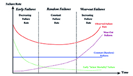
The biggest source of random faults is, however, a fault during manufacturing or wearing out due to ageing. This is represented on the bathtub curve shown in red in Figure 1. This shows the three most important stages of a semiconductor product’s failure rate for a number of devices. For each phase, there is a dominant cause of failures which, when combined, give the red curve with the characteristic bathtub shape.
The initial phase is where early failures are dominant with a high failure rate that rapidly decreases as the devices fail under burn-in test (shown in green) and are eliminated to leave good devices that pass into the second phase. Examples are dust, misalignment of masks and missing bumps. Another example might be ‘test escapes’ where the automated test equipment programme might not have 100% coverage. A very small number of parts might show as passing, but have some manufacturing faults that do not show up. This does not specifically get picked up by stress testing, but some functional testing of the product might find these.
Design for test
An important part of the architectural design stage at the start of a chip project is to consider the design for test aspects so that these are an integral part of the design process from the beginning and not an afterthought further down the line. Part of this is generating the test pattern that will be used to weed out faulty parts at this stage and the failure rate is obviously very high. Very intensive testing can be done by foundries – at a price – to eliminate as many chips as possible that might fail by really stressing them. Foundry TSMC calls this a safe launch.
The failure rate then drops off quickly because the obviously faulty parts have been removed, but some will not have been picked up so early mortality failures continue. The frequency of these continues to also drop off over time – usually well within the first year.

Figure 1: Different failure rates over time
The second phase is random failures with a relatively constant failure rate (shown in blue on Figure 1) that is stable over this period and is also called the service life. The failure rate is measured in failures in time units or mean time between failures (MTBF). Random failures that happen without any indication or warning make them very hard to predict. These are caused by a number of factors such as thermal stress due to the device operating at higher than anticipated temperatures, which can shorten its working life or a manufacturing fault expresses itself by failing.
The third phase is wear-out failures (shown in purple on Figure 1) where the product is failing due to age and wear mechanisms, and the failure rate rapidly increases. Those failure mechanisms are highly dependent on the mission profile (for example, junction temperature or ripple current). Designers need to optimise the design to reduce component stress. For example, a cooling body to effectively reduce the temperature to prolong the lifetime of the component and therefore the system. As a rule of thumb, a 10° increase in the temperature will halve the lifetime of a device.
It is therefore vital to consider the mission profile, that is, the operational conditions for the chip. Long periods of time at very high temperatures will shorten the MTBF so this has to be taken into consideration when ensuring that the parameter for normal life is met. There are numerous standards that define certain qualification tests, which are designed to provoke certain reliability fail mechanisms. In semiconductors, the most used standards are JEDEC
and AEC.
Operational temperature range
The temperature range for most consumer chips is from 0°C to 85°C, while for automotive chips this is extended to -40°C and 150°C because cars are expected to work in the extreme cold of the northern hemisphere and the extreme heat of deserts. Chips in the passenger cabin, such as for infotainment and sat-nav, do not have to be able to withstand the very high temperatures in the engine compartment so the mission profile is vital for the design process.
The mission profile captures the stress that devices will be subjected to over the expected lifetime. It is usually in the form of a table showing times at different temperatures, although this can also show other stresses such as mechanical or humidity. It is needed to estimate if all used devices will be reliable enough to maintain the specified product performance at least over the projected lifetime.
By knowing the mission profile of the temperatures and how they vary over times in situ, a test regime can be mathematically created that mimics the lifetime in use with its challenges to a chip, but condensed into a much shorter time frame.
Functional safety
It is in the middle section of the bathtub curve that random failures occur. By their very nature, these are unpredictable so they are mitigated by ensuring when they fail, they fail safely. In other words, the component can either detect itself that it has failed or other parts of the system detect a failure and take appropriate action. This is a key part of designing for functional safety and requires ‘outside the box’ thinking by designers to compose scenarios where something goes wrong or there is a safety hazard, and the appropriate response.
This is not just a straightforward relationship that has to be considered, as scenarios where two or more events occur concurrently, and which only then trigger a fault, have to be envisaged and planned for. Engineers have to try every possible event and combination of events to see if that triggers a fault. This is, of course, impossible, so planning for a response for the ‘unknown unknowns’ ensures safety is maintained.
ISO 26262 is the standard for any safety system in a vehicle, not just chips. It covers how chips should be designed and tested. Certification that ISO 26262 is achieved can be provided by a third party, such as TUV, for a fee if required, though, in the case of most automotive companies, the internal quality assurance department does rigorous due diligence that is usually in excess of ISO 26262. Design houses should provide detailed records for customers to check that it has complied to ISO 26262 standards throughout design and manufacture.
AEC-Q1 standards
There are currently five key AEC-Q stress test standards that apply to different components. AEC-Q100 covers stress test qualification for integrated circuits, AEC-Q101 is for discrete semiconductors, AEC-Q102 for optoelectronics, AEC-Q200 for passive components and AEC-Q104 for multichip modules.
There are also AEC-Q100 grades that relate to the operational temperature range of the mission profile. These start with Grade 3 for use at -40°C to 85°C, Grade 2 (-40°C to 105°C), Grade 1 (-40°C to 125°C) and Grade 0 (-40°C to 150°C) for chips in the engine bay, for example.
 There are many more aspects to AEC-Q100 covering production, assembly and test regimes. A design house will provide customers with all the documentation to prove that it has met the requirements of the appropriate standard.
Working closely with customers at the architectural design stage for complex automotive chips can ensure that the right balance of power, performance and area (PPA) is achieved while addressing its functional safety and mission profile requirements. The design house may also take a holistic view of the entire value chain right through to shipping silicon so that crucial issues such as testing regimes to the appropriate standards are factored in, together with the increasingly important aspect of packaging. If the latter is very advanced to meet challenging conditions in the engine bay, its costs can exceed that of the chip itself.
Reference architectures designed for automotive use and the ISO 26262 compliance process can fast-track automotive projects. Modularly designed reference architectures can support scalability based on requirements and be configured efficiently with the processing capability and power depending on the end use case and the demands of the customer’s software.
Other considerations are the use of advanced semiconductor nodes and a design and supply, turnkey service frees automotive OEMs from the risks of a multi-stage, multi-supplier, supply chain. Close relationships working directly with the major foundries and outsourced semiconductor and test companies can result in an agnostic approach to IP that enables it to select the most appropriate IP, node and foundry for a project to deliver the required PPA.
 Electronics Weekly Electronics Design & Components Tech News


