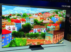
One of the major themes for displays at CES 2024 was the demonstration by a number of vendors of new, large sized MicroLED TVs and signage. Samsung, for example, showcased its range of MicroLED TVs starting at 76in and moving up to a huge 140in models (Figure 1).
MicroLED displays have very small light-emitting elements made from tiny LEDs, typically smaller than 50×50µm. The images they are capable of producing are very bright and colourful, with amazing contrast (the ratio of fully lit to fully off), strong viewing angles and a long operating lifetime, with none of the burn-in problems that have affected OLED TVs. Although the stunning visual performance represents the future of display technology, they are very expensive, with quoted prices typically more than $100,000 for a large signage display.
The size of the MicroLED emitters used is shrinking at quite a pace in order to reduce cost. Back in 2020, each of the emitters were 125×225µm for the red, blue and green sub-pixels in the first variants of the TV technology. In 2024 one of the key suppliers of MicroLEDs to Samsung is talking about 12×27µm emitters, a reduction in LED area of more than 98.8%. Given that the emitters themselves are around 30% of the cost of the overall TVs, this is an important development. It will mean that the cost of future MicroLED displays should start to fall rapidly. It also means that the emitters no longer become the key cost constraint: this now becomes the backplane, the network of transistors that determine the brightness levels of each of the red, green and blue sub-pixels.
Driving MicroLED large displays
MicroLEDs have a very particular response of colour to current density. They require between 1A and 10A per cm2 (an amount that varies between the colours), and a current that increases as the dies get smaller geometrically. The specific brightness and colour drops off rapidly if the current delivered is not at its optimal peak level, a process called droop.
MicroLED displays are premium displays so they require accurate colour performance, and for Samsung this means at least 12 bits of colour depth. As a result of the droop behaviour of MicroLEDs, a mixture of PAM (pulse amplitude modulation) and PWM (pulse width modulation) is needed to drive MicroLEDs. Current architectures for this include a mixture of CMOS MicroIC driving architectures with low temperature poly silicon (LTPS) display backplane technology. This is a high mask count, complex backplane that is able to control the different emitters in both amplitude and pulse width. This LTPS backplane is now becoming the cost and technology constraint for future MicroLED displays.
LTPS fabs are typically limited to around Gen 6 substrates (1,500×1,850mm) with older fabs typically being much smaller than this. To manage yield effectively, MicroLED TVs are made up from tiled smaller LTPS panels, giving the manufacturer an option to offer modular displays of different sizes from 6×6 sub-tiles to 11×11 arrangements. These tiles need to have invisible borders so that the seams are not seen in the final display. This means the backplane driver ICs are wrapped around the back of the LTPS tiles in a process called wrap-around-edge (WAE). This process, however, is also low yield and costly.
Overall, LTPS would not be the choice if designing a large high-performance display starting with a blank piece of paper. A backplane of choice would be monolithic, flexible, potentially transparent, would not need WAE and would be lower in cost and with a lower mask count. It would be manufacturable on a display line larger than Gen 6, and potentially on older Gen 8 or larger lines that already exist.
OTFT pixel on top of MicroLEDs
In ‘Wafer-scale organic-on-III-V monolithic heterogeneous integration for active-matrix micro-LED displays’ (published in Nature Communications), the authors put forward a new strategic option – organic thin-film transistors (OTFTs) to provide a new route to addressing MicroLED displays. The article lists benefits as being a route to monolithic layout, elimination of LTPS tiling constraints and high cost, elimination of WAE, the ability to use larger scale fabs, the ability to do flexible and transparent options and a much lower cost.
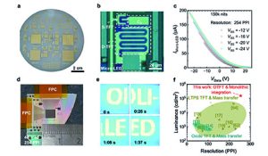
Figure 2: OTFT on top of a MicroLED (Source: Smartkem, Nature Communications)
The architecture is based on turning everything upside down, literally. The MicroLEDs are put emitting side down on an adhesive surface and then the driving transistors are processed at low temperature (< 150°C) on top of the MicroLEDs (Figure 2). Simple interconnections are possible directly to the pads of the MicroLEDs.
OTFT technology status and challenges
OTFT technology uses solution processable organic semiconductor materials. These are a class of new green, low temperature processable (<150°C) materials that offer the display industry new strategic options. For this application the work to date has been based on OTFT on top of semiconductor wafers at 254dpi resolution monochrome displays. Here, OTFT drives enough current for over 100,000nits (Cd/m2) brightness. Typical TVs used in the home operate at around the 700-1,000nits (with the best-in-class OLED or QD OLED displays peaking out at about 2,000-3,000nits). Therefore, OTFT-driven MicroLEDs are very bright, so much so that similar architectures could be used as backlights to an LCD where 96% transmission losses through the LCD are commonplace.
Moreover, OTFT technology can be processed at a reasonable mask count on most display mass production lines, and on a range of substrates that can include a wide choice of optically clear plastics. For OLED today, colourless poly-imide, which actually has a slight yellow tinge, is the substrate of choice due to its high temperature resistance. Processing can go up to 400°C for some of the plasma-enhanced chemical vapour deposition steps of the LTPS backplane process. OTFT could be used with a range of other substrates from type allocation code to polyethylene terephthalate and polyethylene naphthalate. with better cost and colour performance, for novel conformal applications, for example, in automotive display use.
Smartkem produced a first demonstrator based on 254dpi monochrome blue microLEDs (20µm square) which emitted 100,000nits. Work is continuing on 508dpi monochrome and 200dpi RGB implementations using blue emitters and quantum dot colour conversion.
The key point is that OTFTs remove the constraints of today’s modular, LTPS-based MicroLED TVs and signs, opening up options for monolithic implementation, at lower mask count, on transparent, flexible substrates. Backlighting applications for LCDs are possible given the peak current performance of the OTFTs.
Work is being done to move from wafer-based implementations to those based on chip-on-carrier or chip-on-substrate, as well as work to prove that OTFT can be fast enough to cope with the frame-rate pre-charge issues associated with high-colour depth PAM+PWM displays.
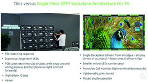
Figure 3:
Steps enabling monolithic MicroLED signage
There are some proprietary planarisation materials that can be highly effective as redistribution layers for mini and MicroLED applications.
There are evolving bottlenecks and technology challenges inherent in MicroLED displays. MicroLED emitter sizes have already begun to fall substantially, so much so that the next architectural constraint will be about the backplane and driving of these displays. Current LTPS modular designs with WAE are expensive and cumbersome while OTFT technology opens up new design space by allowing transistors to be built on top of the MicroLEDs, at lower temperatures and on a range of new, more transparent, plastic substrates.
Display manufacturers will have new options, especially for conformal displays, for example in automotive dashboard applications, and the capability to move to monolithic, cheaper displays with smaller die. OTFT technology can drive 100,000+ nits from standard GaN blue LEDs at 20×20µm and are very suitable for this application.
 Electronics Weekly Electronics Design & Components Tech News
