Despite the fears that Moore’s Law has finally reached its end, the microelectronics sector has adapted to new physical constraints and product requirements through sustained innovation and creativity. A major portion of that creative energy has gone into the development of analogue, RF and mixed signal blocks as embeddable intellectual property (IP).
The selection of analogue/RF/mixed signal IP is both broad and deep. One can find a multitude of hardware blocks in 7nm (and in some cases even 5nm) for PLL and DLL, DACs and ADCs (available with resolutions of 8- to 24‑bit and up to 300Msamples/s). There are are also PHYs and SerDes, targeted at wireless, networking, computing and memories.
There are also smaller components that can be assembled to create personalised analogue front ends (AFEs), power management functions and RF modules.
The industry has produced a steady stream of process technology advances to support the demand for higher gate counts, lower power, greater performance and increased functionality, including triple well isolation, silicon on insulator (SoI), P+ guard rings, finfet and trench isolation.
As well as contributing to the proliferation of analogue/RF/mixed signal IP, these substrates have reduced the magnitude of some of the deep sub‑micron, for example analogue noise sources hidden in slew rates, impedance matching and termination complications, and circuits that support tremendous bandwidths.
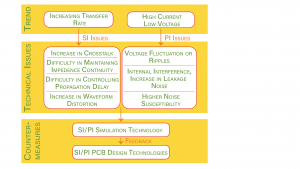
Yet even novel process enhancements are coming up short in the face of massive gate counts placed side by side with analogue circuitry in SoC designs of 16nm and below. The signal and power integrity challenges presented by large, high performance digital blocks in close proximity to analogue/RF macros are spreading from chips into packaging and PCBs.
Silicon practices
Analogue circuitry is decidedly sensitive to how circuits are placed and routed. Design rules (eg. trace and via pitch, differential signalling, extra ground pins) help to avoid, or at least reduce, substrate coupling and proximity effects that result in EMI problems, which is why design rule checks (DRC) are part of the physical verification effort after layout.
Layout versus schematic (LVS) checking is also part of verifying intended connectivity. Parasitic extraction directly affects identification of further potential sources of coupling, with back annotation of parasitics often resulting in schematic and layout changes. Unfortunately, this will in turn affect timing, dynamic range, load, gain and power, as well as generating a fresh new set of parasitics. Iterative loops which return to the beginning of the design flow are a tragic necessity, which is why analogue design is considered to be much more of an art than a science.
Integration of the resultant analogue block(s) into the overall asic/SoC design presents a whole new host of concerns.
For both digital and analogue circuit blocks, chip floor‑planning will be constrained by the optimal location of each block, pin placement, I/O locations, critical paths, power and signal distribution, the size of the chip and its aspect ratio. Analogue IP is particularly sensitive to most of these issues, and the fact that analogue blocks are also hard macs complicates further.
Once a chip’s blocks are placed, best routing practices include implementing all critical paths first, whether analogue or digital. When it comes to non‑critical paths, analogue signals should take precedence.
All analogue routing requires special consideration in terms of matching parasitics, minimising coupling effects and avoiding excessive IR drops. This is accomplished by employing shielding techniques, keeping traces short, routing return signal paths by the most direct route and differential signalling.
Different categories of analogue circuitry may need particular attention. For example, there are considerations when using a DAC or ADC beyond its resolution and sampling rate. Following Nyquist’s sampling theorem can cause bandwidth, power and bit synchronisation challenges for very high performance applications.
Wireless is problematic from a sampling point of view, while audio is generally the most demanding in terms of resolution. This is where a parameter such as the effective number of bits (enob) has particular relevance. No matter what the advertised resolution, pushing such a block past its enob will degrade its SNR performance with potentially significant consequences to the usefulness of the block.
Above and beyond all this is the fact that analogue block design and integration into the context of an SoC or asic is simply not as ‘clean’ and predictable an engineering effort as the digital section of the chip. As the dimensions of SoC design work expand, design teams will need to grow their skill sets and practices.
Package considerations
Capacitive coupling in SoC design can be dealt with at the silicon level, but it also manifests itself in packaging.
Coupling can be observed between signal traces, whether or not both are active, and can even come from the power bus.
One frequently observed problem is analogue/RF circuits becoming a source of EMI for digital blocks, causing inter‑modulation with frequency summing and harmonics at both low and high frequencies. Sharing package ground and power planes between analogue/RF and digital blocks can expose analogue circuitry to digital switching noise, major current spikes and coupling through poorly implemented return paths. Equally, tying analogue and digital ground pins together risks forming a loop antenna that will both attract and generate noise.
Keeping source and return paths physically close avoids current loops, although there are other SoC‑caused problems. Some packages have included native inductors as de‑coupling components to save space. Power integrity issues mean that transmission lines have been used to supply power in some applications.
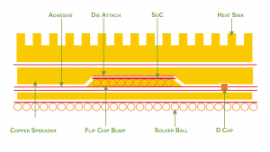
The proliferation of multi-chip devices – system in package, wafer scale integration and 2.5D/3D ICs – mean that die can be specialised as analogue, digital or memory modules and then stacked, with through‑silicon vias providing connectivity between metal stacks and interposers aggregating signal and ground pins to interface with package balls and the PCB. With the appropriate design rules for through silicon via (TSV) distancing and signal/ground distribution, 2.5/3D ICs go a long way towards resolving many signal and power integrity issues for ultra‑deep sub‑micron SoC.
2.5/3D IC is perhaps 2‑3% of the semiconductor market but it is growing energetically, and might triple in size over the next five to six years.
PCB issues
Basic electrical issues such as dielectric loss, dissipation factor and skin effect, are noticeable in PCBs, from massive current dumps that destabilise the ground reference for analogue circuitry. Gb/s of data rates creates more severe crosstalk and inter-symbol interference (ISI). Vdds for analogue/RF and digital blocks also contribute to EMI problems; even clock signals can become a source of EMI because of the frequency and edge rate.
Layered PCBs afford greater size and depth compared to packages. Implementing separate analogue and digital ground planes to avoid current‑based EMI issues between the two types of circuits can create a dipole antenna in the board. Connecting separate ground planes with traces in order to ameliorate such a problem often leads to generating another antenna.
The EMI potential of a chip or circuit is not always sufficient to assess the risk of noise. High precision ADCs, for example, are more accurately evaluated for EMI not by their Fmax, but by their sampling rate.
A long‑standing practice of board designers is to separate analogue and digital components on a board and allow only DACs or ADCs to straddle the boundary between them. In addition, digital and analogue signal traces are segregated to their own regions – passing one through another’s domain is studiously avoided. Finally, it is considered imperative to not cross an analogue or digital trace over the other.
Crossing analogue and digital signal traces or passing one kind of signal trace through the other’s domain cannot be evaded. Making sure the design rule violation occurs above a ground plane reference safeguards against crosstalk through induction.
Clean partitions between analogue and digital signalling domains on PCBs are almost impossible. SoCs contain both analogue/RF and digital circuits and can only rarely be placed on the board across domain boundaries as ADCs and DACs are. Even chips that appear entirely digital in function can have a small embedded analogue component, such as a DSP with an internal PLL.
As a rule, PCB designers will ground mixed signal devices to the same grounding plane as they do purely analogue components, but for chips with a relatively small analogue component, it can get trickier. Chip vendors often provide separate ground pins and instruct board engineers to bring both pins to the digital ground reference plane. This may require a de‑coupling cap to be placed with the analogue ground pin. Tying the analogue and ground pins together brings the trace to analogue ground by the shortest distance.
One advantage PCBs have over chips and packages is the ability to deploy large, thick copper ground planes. They provide a consistent impedance across a wide frequency range, reduce components and help with thermal conductivity.
To prevent large transient currents from travelling across such a ground plane from high frequency digital switching activity, board designers divide the plane into a digital and an analogue portion. These separate planes can be connected using Schottky diodes or other high impedance methods to prevent transient voltage building up while simultaneously blocking current spikes from crossing between them.
EDA and PCB companies can both provide additional expertise, and there are continual efforts to develop improved dielectric materials for board layers that are superior insulators while still being cost effective and manufacturable.
A broader design view
Arising from the view that IP integration problems are due to design methods which do not treat chip, package and PCB design as a whole, the concept of a power distribution network (PDN) has arisen.
Using the generic formula ‘Z = delta V (power supply noise)/I’, the Z parameter can be estimated from the transistor current draw I, which is assumed to be a constant. This serves as an upper limit for all three levels of the system across the full range of operating frequency.
Z will vary based on individual resistance, inductance, capacitance (RLC) and operating frequency. The upper limit will be dominated by resistance and inductance and the lower by capacitance at any given resonant frequency. What the RLC values are at each level will depend on that level’s ground plane, use and dimensions of bulk or de‑coupling capacitors, pins, traces.
The commonalities in EMI sources produce universal problems. For example, current return paths with discontinuities are a common source of EMI. These are managed with de‑coupling caps, although insulating materials composed of thin or high permittivity dielectrics are also used.
TSVs and through mould vias (TMVs) in packaging have become a potential source of crosstalk at all three levels.
Proper spacing, scattering ground vias between signal vias, differential signalling and shortest distance to ground references are all used to mitigate the problem. Heavy use of de‑coupling caps will affect floor planning, layout and design choices and cost. Current changes from inductive parasitics will be dependent on current draw at the chip level and can instigate more current draw from an on-chip voltage regulator. This is highly undesirable, as on‑chip regulators are a source of parasitic capacitance. In this case, de‑coupling caps serve as ‘rechargeable batteries’ that even out current flows.
Convergence
In order to properly integrate system IP in silicon, chip developers must, in effect, become system developers.
This is turning into a requirement for chip design teams to expand their skills in order to encompass co-development at the chip, package and board level during the full modelling, design, simulation and verification cycle.
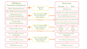
An essential addition to a co‑design work flow (Figure 4) would be to incorporate prototyping of each level of abstraction, including trial layouts, physical prototyping to low or zero levels of abstraction as logic design is completed. By engaging in co‑design between all three levels dynamically from the outset, IP integration issues can be addressed by cycles of planning and optimisation before final tape‑out.
Regardless of the effectiveness of an EDA tool or design flow, it is clear that it is no longer sufficient to design a chip and integrate its digital and analogue IP, then optimise die placement in a chosen package and in turn optimise its placement on a multi‑layer PCB. Engaging each level independently will lead to significant cost over-runs, delays and re-engineering.
The integration of semiconductor digital and analogue IP can only be timely and efficient when the chip design team accounts for the ‘vertical’ dimension of the SoC and includes detailed packaging and PCB parameters in design, simulation and verification flows, treating the three levels as one system.
 Electronics Weekly Electronics Design & Components Tech News
