Advancing microscopy for electronics inspection
Microscopes have formed an integral part of electronics inspection for decades, and are used along the supply chain to check that finished products or individual parts are within specifications. And as products and specifications have evolved, so have modern industrial microscopes. The latest inspection microscopes combine superb resolution and image quality smart features that fulfil the requirement of modern QC – for example measurement capabilities, traceability and ease of use.
The changing face of PCB production
In many electronics inspections, for example in the manufacture of printed circuit boards (PCBs), roughness plays an important and changing role. Production of PCBs has always relied on low-roughness copper, but as we enter the age of 5G, specifications are becoming more stringent.
These tighter specifications result from the fact that signal transmission strength changes in materials with high roughness as the frequency of the signal changes. As a result, materials that have acceptable transmission properties at 4G frequencies (<3.5 GHz) might struggle when used in 5G applications (>3.5 GHz).
High roughness causes signal loss at high frequencies due to the skin effect (figure 1). At lower frequencies, the signal flows through the whole circuit, which means that there is little need for considering surface signal loss. At higher frequencies, however, the signal flows mainly near the surface and roughness will become more important.
Figure 1. Surface properties become more important in transmission strength at high frequencies.
Rough? Rougher? Rough-ish?
For many inspection parameters, definitions are straightforward and measurement is relatively easy. In the case of roughness however, it is easy to get an intuitive understanding of rough and smooth surfaces, but defining parameters that can be used to set a reliable cutoff value for roughness is challenging.
Inspectors can assess surface roughness in many ways, but most detailed methods rely on acquiring a high-resolution 3D map of a specimen first. These maps offer more detailed information than line profile methods and are also easier to interpret. Inspectors can create these maps using multiple technologies, but confocal microcopy is particularly well suited to the needs of high-throughput electronics inspections.
Zooming in on roughness
Offering submicron precision, industrial confocal microscopes are the most accurate and precise microscopy method for looking at surfaces. They measure the shape and roughness of surfaces at the submicron level without affecting the surface in any way. Confocal microscopes also capture data of rough surfaces more accurately than alternative techniques such as white light interferometry due to their high lateral resolution.
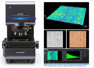
Olympus’ LEXT OLS5100 confocal microscope (figure 2) combines these benefits with easy setup and simple operation. The LEXT measures roughness parameters with a resolution below 5 nm – exceeding the standards for ISO 25178 – and provides smart scanning algorithms for improved throughput and smart tools that make the microscope easy to use. This combination makes it well suited for electronic inspections – not just in PCB manufacturing but also in inspection of, for example, electrodes of batteries or memory cards.
Figure 2. Industrial confocal microscopes, such as Olympus’ LEXT OLS5100, offer sub-micrometer resolution in roughness measurements.
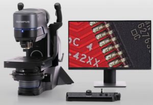
When more versatility is required, for example when using one microscope for a variety of different electronics inspections, digital microscopes are a good alternative. Compared to conventional microscopes, digital microscopes have the benefit of displaying images of a specimen directly on-screen without the need for oculars. The Olympus DSX1000 digital microscope (figure 3), for example, helps inspectors by showing specimens under six different observation methods at all magnifications. It also features objectives that have long working distances, high resolution and can be exchanged in seconds. Its telecentric optical system, which avoids parallax and other distortions from occurring when adjusting the focus, means that the microscope provides accurate measurements, even at micrometer scales.
Figure 3. For high versatility with reliable, micrometer-scale measurements, the Olympus DSX1000 offers a highly suitable system for electronics inspections.
Precision and versatility
In electronics manufacturing, inspection takes place along a product’s supply chain, but the detailed specifications of inspections are subject to constant change as new technologies, methods and applications emerge. Specialized industrial microscopy systems, such as confocal and digital microscopes, are excellently placed to tackle these challenges. By combining high-precision and measurement capabilities with the versatility to support multiple inspection workflows, they help inspectors across the industry to have confidence in every component.
For more information on microscopes and measurement you can visit the Olympus Advanced Optical Metrology Hub. Here, you’ll find useful ebooks and webinars on metrology, for example this presentation by Dr. Uwe Brand of the German National Metrology Institute (PDB) in Braunschweig on 3D roughness and dimensional measurements.
And if you are an academic researcher with a passion for excellence, looking to collaborate with other experts and industry professionals, then you might be interested in joining our new community – Olympus LINKS – to drive microscopy forward and collaborate to find the answers to the challenges of tomorrow.
Author
Markus Fabich is the strategic marketing manager for industrial equipment at Olympus Europa and has been a member of the European for almost 17 years. Starting in the service team as an engineer responsible for advanced laser-based systems alignments and calibrations, he has now been working for 10 years as a part of the product marketing team, introducing innovative equipment to the European market starting from the OLS3000 confocal microscope and headed various programs like the Olympus Technology Grant.
 Electronics Weekly Electronics Design & Components Tech News


