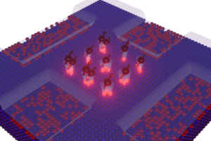
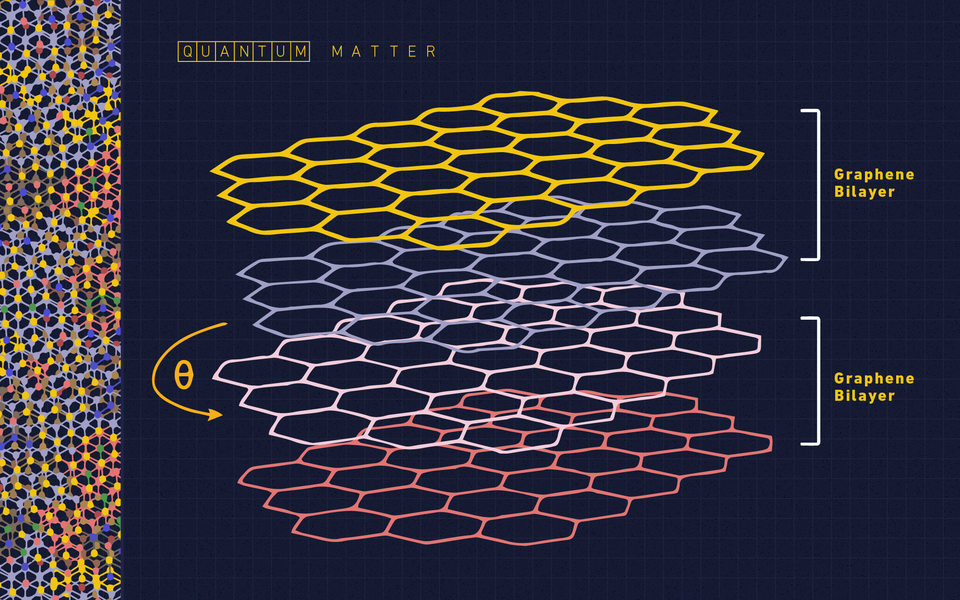
When two or more overlying sheets of graphene are slightly misaligned — twisted at certain angles relative to each other — they take on a plethora of exotic identities.
Depending on the twist angle, these materials, known as moiré quantum matter, can suddenly generate their own magnetic fields, become superconductors with zero electrical resistance, or conversely, turn into perfect insulators.
Joseph A. Stroscio and his colleagues at NIST, along with an international team of collaborators, have developed a “quantum ruler” to measure and explore the strange properties of these twisted materials.
The work may also lead to a new, miniaturized standard for electrical resistance that could calibrate electronic devices directly on the factory floor, eliminating the need to send them to an off-site standards laboratory.
Collaborator Fereshte Ghahari, a physicist from George Mason University in Fairfax, Virginia, took two layers of graphene (known as bilayer graphene) of about 20 micrometers across and twisted them relative to another two layers to create a moiré quantum matter device.
Ghahari made the device using the nanofabrication facility at NIST’s Center for Nanoscale Science and Technology. NIST researchers Marlou Slot and Yulia Maximenko then chilled this twisted material device to one-hundredth of a degree above absolute zero, reducing random motions of atoms and electrons and heightening the ability for electrons in the material to interact.
After reaching ultralow temperatures, they examined how the energy levels of electrons in the layers of graphene changed when they varied the strength of a strong external magnetic field.
Measuring and manipulating the energy levels of electrons is critical for designing and manufacturing semiconductor devices.
To measure the energy levels, the team used a versatile scanning tunneling microscope that Stroscio designed and built at NIST.
When the researchers applied a voltage to the graphene bilayers in the magnetic field, the microscope recorded the tiny current from the electrons that “tunneled” out from the material to the microscope probe tip.
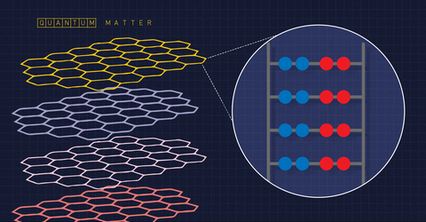
In a magnetic field, electrons move in circular paths. Ordinarily, the circular orbits of the electrons in solid materials have a special relationship with an applied magnetic field: The area enclosed by each circular orbit, multiplied by the applied field, can only take on a set of fixed, discrete values, due to the quantum nature of electrons.
In order to maintain that fixed product, if the magnetic field is halved, then the area enclosed by an orbiting electron must double.
The difference in energy between successive energy levels that follow this pattern can be used like tick marks on a ruler to measure the material’s electronic and magnetic properties.
Any subtle deviation from this pattern would represent a new quantum ruler that can reflect the orbital magnetic properties of the particular quantum moiré material researchers are studying.
In fact, when the NIST researchers varied the magnetic field applied to the moiré graphene bilayers, they found evidence of a new quantum ruler at play.
The area enclosed by the circular orbit of electrons multiplied by the applied magnetic field no longer equaled a fixed value. Instead, the product of those two numbers had shifted by an amount dependent on the magnetization of the bilayers.
This deviation translated into a set of different tick marks for the energy levels of the electrons. The findings promise to shed new light on how electrons confined to twisted sheets of graphene give rise to new magnetic properties.
“Using the new quantum ruler to study how the circular orbits vary with magnetic field, we hope to reveal the subtle magnetic properties of these moiré quantum materials,” Stroscio said.
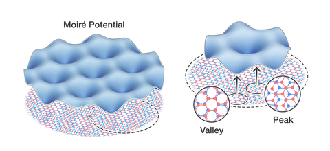
In moiré quantum materials, electrons have a range of possible energies — highs and lows, shaped like an egg carton — that are determined by the electric field of the materials. The electrons are concentrated in the lower energy states, or valleys, of the carton.
The large spacing between the valleys in the bilayers, bigger than the atomic spacing in any single layer of graphene or multiple layers that aren’t twisted, accounts for some of the unusual magnetic properties the team found, said NIST theoretical physicist Paul Haney.
The researchers, including colleagues from the University of Maryland in College Park and the Joint Quantum Institute, a research partnership between NIST and the University of Maryland, described their work in the October 6 issue of Science.
Because the properties of moiré quantum matter can be chosen by selecting a specific twist angle and number of atomically thin layers, the new measurements promise to provide a deeper understanding of how scientists can tailor and optimize the magnetic and electronic properties of quantum materials for a host of applications in microelectronics and related fields.
For instance, ultrathin superconductors are already known to be exquisitely sensitive detectors of single photons, and quantum moiré superconductors rank among the very thinnest.
The NIST team also has an interest in another application: Under the right conditions, moiré quantum matter may provide a new, easier to use standard for electrical resistance.
The present standard is based on the discrete resistance values that a material takes on when a strong magnetic field is applied to the electrons in a two-dimensional layer.
This phenomenon, known as the quantum Hall effect, originates from the same quantized energy levels of the electrons in the circular orbits discussed above. The discrete resistance values can be used to calibrate the resistance in various electrical devices.
But because a hefty magnetic field is needed, the calibrations can only be conducted at a metrology facility such as NIST.
If researchers could manipulate quantum moiré matter so that it has a net magnetization even in the absence of an external applied magnetic field, Stroscio said, then it could potentially be used to create a new portable version of the most precise standard for resistance, known as the anomalous quantum Hall resistance standard.
Calibrations of electronic devices could be performed at the manufacturing site, potentially saving millions of dollars.
 Electronics Weekly Electronics Design & Components Tech News
