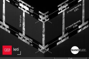
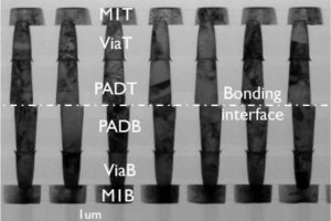
French research lab CEA-Leti has reported stacking three 300mm wafers for improved CMOS image sensors, using hybrid wafer bonding and high-density through-silicon vias. The announcement was made in three papers at ECTC, the 2024 IEEE Electronic Components and Technology Conference in Colorado. 6μm hybrid bonding pad pitch, and TSVs are 1 x 10μm It is working towards a new generation ...
Tag Archives: 300mm wafers
400nm pitch wafer-bonded conductors for memory-on-logic ICs
Semiconductor research lab Imec has demonstrated wafer-bonding with 400nm pitch copper conductors across the boundary, proposing the technology for logic-on-logic and memory-on-logic wafer stacking within ICs, and for adding back-side power networks to die. Top and bottom wafers bonded by contact at room temperature, and then annealed. Migrating from the usual square array of wafer-to-wafer interconnects, these are in a ...
CEA-Leti and Intel put 2D materials on 300mm wafers for nano-sheet transistors
Intel is to team up with French lab CEA-Leti to put two-dimensional transition-metal dichalcogenides on 300mm wafers. The aim of the multi-year project is to develop a way to transfer layers of 2d material, grown on substrates up to 300mm, to a second substrate for transistor building. Intel will supply manufacturing expertise and CEA-Leti has bonding, layer-transfer and characterisation knowledge. ...
TI second 300mm fab in Utah
Texas Instruments is to build its next 300mm wafer analogue and embedded processor fab in Utah, next to its existing 300mm fab in the town of Lehi. Once completed, the Lehi fabs will operate as a single unit. “This new fab is part of our long-term, 300mm manufacturing roadmap,” TI COO Haviv Ilan. “With the anticipated growth of semiconductors in ...
Infineon opens thin wafer power fab
Earlier today, Infineon opened its fab for power electronics on 300mm thin wafers at its Villach site in Austria. At €1.6 billion, the investment made by the semiconductor group represents one of the largest such projects in the microelectronics sector in Europe. The Villach site is one of the world’s most modern fabs and was opened by Infineon CEO Reinhard ...
More on: Making MEMS on 300mm wafers
French research fab CEA-Leti has begun manufacturing accelerometers on 300mm wafers, thought to be a first for the MEMS industry. “This demonstration that our 200mm MEMS platform is now compatible with 300mm wafer fabrication shows a significant opportunity to cut MEMS production costs,” said Leti CEO Marie Semeria. “This will be especially important with the expansion of the Internet of things and ...
23 more 300mm fabs by 2019, says IC Insights
By 2019 there should be 110 volume production 300mm fabs in the world compared to 87 today, reports IC Insights. The number of 300mm fabs will likely peak between 115-120. By comparison, the greatest number of volume-production 200mm wafer fabs in operation was 210 (the number declined to 154 fabs at the end of 2014). The list of companies with ...
Intel goes green with Arizona Fab32 for 45nm ‘Penryn’ chips
Intel has officially begun production for 45nm desktop, laptop, and servers processors at its manufacturing factory in Chandler, Arizona, dubbed Fab32.
Fabs not required for success
Although some believe “real men have fabs”, owning a fab no longer appears to be a prerequisite
Welsh wafer firm doubles revenues
Pure Wafer's interim results, the first since floating, show turnover more than doubling to £3.98m
 Electronics Weekly Electronics Design & Components Tech News


