Intel has put a lot of money and effort into packaging. In the last seven months it has announced investments of $10 billion in its Rio Rancho and Penang packaging plants.
At IEDM it described its approach to the upcoming packaging generation – copper hybrid bonding interconnect – which takes over when bump dimensions get to below 10 micron and delivers a 10x improvement in interconnect density.
Intel calls its version Foveros Direct. It delivers direct copper-to-copper die-to-die bonding for low-resistance interconnects between tiles to increase the capabilities of chiplets,
The technology is scheduled for deployment in 2023. Others, including Samsung and TSMC, are pursuing the same approach and may start using hybrid bonding interconnect before Intel.
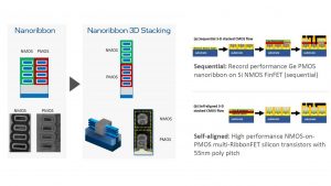
On scaling, Intel is putting its faith in stacking multiple GAA CMOS transistors in what it calls its RibbonFET process technology to achieve a 30%-50% increase in transistors per silicon area.
Looking further into the future, Intel is working on 2D transistors. “2D CMOS transistors fabricated with transition metal dichalcogenide (TMD) materials are a potential replacement for silicon transistors at sub-12nm channel length,” says an Intel IEDM paper, “TMD transistors have a promising future as a CMOS replacement technology because TMDs do not suffer from channel scaling issues that limits Si transistors In sub12-15nm LGSi CMOS, the Si channel needs to be aggressively scaled, which degrades the on-state mobility. 2D FETs do not suffer these intrinsic effects since their body thickness is already sub 1nm without mobility loss relative to their bulk values.”
Another look into the future at IEDM was a paper on GaN-on-Si technology which, says Intel “sets the stage for low-loss, high-speed power delivery to CPUs while simultaneously reducing motherboard components and space.”
The IEDM paper makes a series of claims for its GaN-on-Si capabilities saying It demonstrates “scaling of an enhancement-mode (E-mode) high-k GaN-on-300mm Si(111) NMOS transistor achieving best-in-class performance and figure-of-merits for integrated power electronics and RF mm-wave,” write the researchers, “here, we demonstrate many firsts and industry records for GaN-on-Si, including record fT/fMAX of 300/400GHz and transconductance GM>2100μS/μm with industry thinnest TOXE=14.8Å; record high VDS= 65V for a 30nm channel length GaN transistor with excellent RON=495Ω-μm; first truly e-mode GaN achieving full ON-current with record low-gate-drive, VGon=1.8V, IOFF= 25pA/μm at VD=30V (VG=0V); high-Q MIM and inductor enabled by GaN industry’s first 4-metal layer Cu backend interconnect process on 300mm silicon; outstanding RF performance: 24dBm RF output power (VD=10V) and high power density 2.7W/mm at 28GHz; 17.6dBm (0.72W/mm) with PAE=20.1% at 76GHz, and 0.4W/mm with 10.5% PAEand 4.3dB gain at 90GHz.”
Intel is pursuing a number of futuristic opportunities: the use of novel ferroelectric materials for embedded DRAM; silicon transistor-based quantum computing devices and magnetoelectric spin-orbit (MESO) logic devices at room temperature, which could be used for a new type of transistor based on switching nanoscale magnets.
Intel also announced that, working with Imec, it is making progress with spintronic materials research to take device integration research close to realising a fully functional spin-torque device.
 Electronics Weekly Electronics Design & Components Tech News


Memory does not stack well on 250 Watt CPUs. Cutting Watts in half cuts performance in half. Those leaky 10nm transistors need some R&D. Pat Gelsinger is on the case. This week he is transistor shopping in Taiwan where the sign on the door says “Sold Out”.