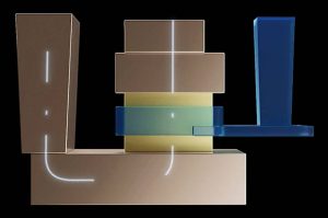
IBM’s VTFET with a vertical channel (yellow) and gate-all-around (blue). Contacts are brown and the white line shows current flow.
It calls them VTFETs, for vertical transport FETs, and is describing the channel cross-section as ‘nanosheet’.
“VTFET nanosheet electrical results show excellent sub-threshold slope and DIBL [drain induced barrier lowering], and symmetric device operation,” according to IBM’s IEDM paper. “At fixed footprint and aggressively scaled gate pitches, VTFET nanosheets can deliver increased device drive due to a combination of good electrostatics, low parasitic losses, and area savings from the use of zero diffusion breaks.”
Modelling, according to the company, shows VTFET logic would be around twice as fast for the same power as finFETs scaled to the same gate pitch, or use 85% less power for the same speed. Part of this comes from having around half the parasitic capacitance of what would be cramped finFETs.
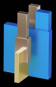 As conventional CMOS transistors have been shrunk, their inherent switching characteristics have got worse.
FinFETs redressed the balance for a while (left). In these, current flow is lateral through the tall thin fin-like channel (yellow). The gate (blue) has access to the sides and top of the channel, and both only have edge-on parasitic capacitance to the substrate below (electrodes are shown in brown).
At the expense of complex fabrication, there are ways to improve finFETs by breaking the fin into a series of bars (no image, but looking like a farm gate) and extending the transistor gate (and its insulator) through the gaps. This creates a ‘gate-all-around’ (GAA) structure for the upper bars where the gate gets complete access to the carriers in the channel from all sides.
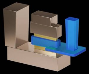 The resulting bars are called ‘nanowires’ and such transistors are ‘nanowire FETs’. If the bars are made wide and flat, they are referred to as ‘nanosheets’, and this is where IBM has borrowed the name for its vertical channel device, which has a long thin footprint (right).
Vertical fets stray even further from traditional CMOS fabrication, but as IBM (and others including IMEC in Belgium) has shown, in tiny transistors where the geometry gets extremely cramped – at the 2nm node, for example – the structure wins on electrostatics and parasitics .
“Vertical-transport nanosheet FETs are a strong candidate for scaling beyond the limits of lateral-transport FET architectures,” said IBM.
Diagrams courtesy of IBM, used with permission.
 Electronics Weekly Electronics Design & Components Tech News

Pat Gelsinger should be in Seoul today instead of Taipei.