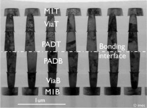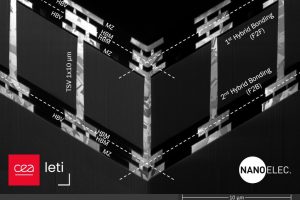
Top and bottom wafers bonded by contact at room temperature, and then annealed.
Migrating from the usual square array of wafer-to-wafer interconnects, these are in a hexagonal pattern for its high-density packing and equidistance between all neighbours.
Equal-sized pads across the interface have been tried (see image) as well as smaller pads on one side – so far unequal copper pads appear to deliver lower parasitic capacitance and higher dielectric breakdown strength.
For acceptable yield, the project has established that better than 100nm alignment has to be maintained across the surfaces of a pair of 300mm wafers as they are brought together – for which a commercial wafer bonder was modified.
Bonding is spontaneous at room temperature if the surfaces have been prepared correctly, with post-bonding annealing to consolidate adhesion.
An optimised chemical-mechanical polishing process has been developed both to flatten the surfaces to the extraordinary degree necessary, and to leave the copper pads a few nanometres below the plane of the dielectric which reduces the chance of voids forming during annealing.
The researchers moved away from silicon dioxide for the dielectric, moving to silicon carbon nitride (SiCN) as it forms a mechanically-stronger bond, blocks copper diffusion and still passivates the wafer by blocking gas diffusion.
Annealing at 250°C is enough to bond the SiCN on one wafer to the SiCN on the facing wafer, and higher temperatures can be tolerated.
The image was first presented at IEDM 2023 in the paper ‘The challenges of Cu/SiCN wafer-to-wafer hybrid bonding scaling down to 400nm pitch’.
 Electronics Weekly Electronics Design & Components Tech News


