The ultra-wide bandgap and high thermal conductivity of AlN is also applicable to RF and power devices.
Its first 100mm AlN wafer was made in August last year, and the company began selling 2inch diameter substrates for RF device R&D in late 2023.
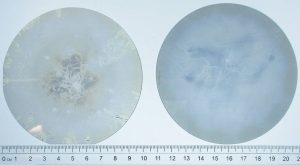
By Q1 this year it had 90% usable 100mm wafers (photo left) and then the 99.3% wafer (right) in Q2.
“This 100 mm diameter milestone accelerates the development of new applications on AlN substrates as it integrates into existing fabrication lines for RF and power devices using alternative materials,” according to Crystal IS. “The company plans to offer 100mm diameter substrates, which will be exclusively manufactured in its US facility, to key partners this year.”
Crystal IS, part of Asahi Kasei since 2011, manufactures at its headquarters in Green Island, New York. It was spun out of Rensselaer Polytechnic Institute in 1997.
 Electronics Weekly Electronics Design & Components Tech News


