Emerging electron pairs in an insulator hint of a hidden mechanism that could be exploited for designer ‘high-temperature’ superconductors. Superconductors need electrons to pair, and then many pairs to become coherent inside the material. “The electron pairs are telling us that they are ready to be superconducting, but something is stopping them,” said Ke-Jun Xu, a researcher at Stanford University’s ...
Tag Archives: oxide
A better amorphous p-channel thin-film transistor
Scientist in Korea are making fast p-channel amorphous thin-film transistors. “Research progress on p-type amorphous semiconductors has been notably sluggish,” according to the Pohang University of Science and Technology (PosTech). “Despite the widespread adoption of n-type amorphous oxide semiconductors, particularly those based on IGZO [indium gallium zinc oxide] in OLED displays and memory devices, the advancement of p-type oxide materials ...
Get high mobility and high stability in display-grade TFTs
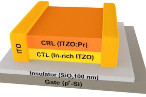
75.5cm2/V/s mobility and high stability are claimed for amorphous oxide semiconductor thin-film transistors created at the Ningbo Institute of Materials Technology and Engineering (NIMTE). The bottom-gate transistor is built with a stack of two layers: Next to the oxide-insulated silicon gate is a charge transport layer (CTL) consists of indium-rich InSnZnO “featuring large average effective coordination numbers for all cations ...
Fast p-type oxide semiconductor rolled into life with liquid metal
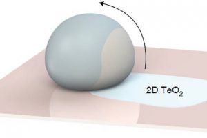
A fast transparent p-type oxide semiconductor is possible, according to scientists in Australia who have turned theoretical tellurium materials into reality using a novel deposition process. Two-dimensional beta-tellurite is the semiconductor, deposited by rolling a bead of molten tellurium and selenium across the substrate. “This high-mobility p-type oxide fills a crucial gap in the materials spectrum to enable fast, transparent ...
Transparent solar cell from simple metal oxides
A transparent solar cell can be made using straight-forward metal oxides, according to researchers at Incheon National University in Korea. The cell converts the ultra-violet portion of the sun’s spectrum into electricity using a junction made from p-type NiO and n-type TiO2 – the latter a well-known photo-electric material. Unlike more exotic transparent solar absorbers, the materials are stable in ...
Passivation pushes gallium oxide transistor to over 8kV
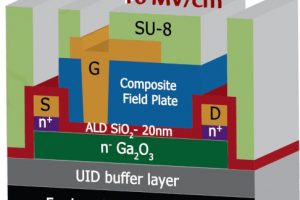
Organic surface passivation has allowed a gallium oxide transistor to hold-off 8.03kV – the highest reported for a lateral mosfet, according to the University of Buffalo engineering team behind the device. The proof-of-concept device was passivated with the high field strength epoxy polymer SU-8. Without passivation, a similar transistor scored 2.7kV. This un-passivated voltage is also remarkable, as the same ...
Oxide transistor printed around 2mm tube, for medical diagnosis
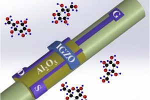
Transparent transistors have been fabricated around glass tubes of 2mm diameter, at Oregon State University. It replaces a polymer transistor, printed on film and wrapped around the tube, which fell apart when tested as part of an artificial pancreas – a catheter intended to detect blood sugar levels and transmit the information to a wearable insulin pump for diabetics. Key ...
2-d hole gas finally demonstrated
Two-dimensional electron gas clouds are used in electronic devices – they are the reason GaN transistors conduct so well. But where is the long-postulated two-dimensional hole gas? The answer is: it is where Professor Chang-Beom Eom and his team made it, at the University of Wisconsin-Madison. “The 2D hole gas was not possible primarily because perfect-enough crystals could not be ...
Flexible circuit is only 4μm thick
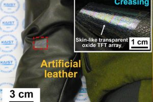
Complete with substrate, an active matrix for a flexible display need only be 4μm thick, according to the Korea Advanced Institute of Science and Technology (KAIST). The matrix of ultra-thin n-type transparent oxide thin-film transistors (TFTs) for the backplane were initially fabricated on a sacrificial laser-reactive substrate. Laser irradiation from the backside of the substrate split off only the oxide ...
 Electronics Weekly Electronics Design & Components Tech News


