Automotive ICs are increasingly developed and manufactured using cutting-edge processes. These devices are no longer only deployed for simple functions like controlling windows or light signaling but are now required for complex functions related to advanced driver-assist systems (ADAS) and increasingly for autonomous driving applications. The processing power required for these advanced functions results in the need for very large and complex ICs manufactured for optimal power efficiency. This, coupled with the need for these devices to meet the stringent safety requirements of the ISO 26262 standard, is resulting in a new set of challenges for automotive device and systems manufacturers. Solutions are needed to ensure new complex automotive electronic systems operate safely at all times throughout the life of the vehicle. This is known as functional safety.
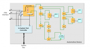
Functional safety relies on mechanisms within the design, referred to as safety mechanisms, to be able to monitor and check for the correct functional operation of the design whilst it is use. The ability of the these safety mechanism to cover potential faults both latent and transient will determine the overall diagnostics coverage of the design driving the level of ASIL that can be achieved. An approach that is extremely popular is to make use of a set of embedded monitoring functions distributed throughout each semiconductor device and tied together through a global communication infrastructure that enables rapid detection and reporting of random failures anywhere in the system. The monitors must operate without interfering with normal functional operation and have the flexibility to provide varying degrees of failure coverage based on the end-application of the semiconductor device and the associated Automotive Safety Integrity Level (ASIL) classification. An example chip-level test architecture supporting distributed system-wide monitoring is illustrated in Figure 1.
Figure 1: Chip-level test architecture for in-system test
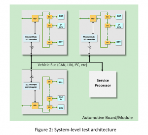
A standard IEEE 1149.1 test access port (TAP) provides a portal to all on-chip test resources for manufacturing test. The TAP connects to a reconfigurable serial access network based on the IEEE 1687 standard (often referred to as the IJTAG standard). This IJTAG network is made up of switches called segment insertion bits (SIBs). Each SIB allows a sub-network to be switched-in or bypassed, allowing for optimized access to any test resource within the network. The IJTAG network is also accessed by an In-System Test (IST) controller. The IST controller communicates through a CPU interface to either the outside world or an internal safety manager and performs the parallel to serial and serial to parallel data conversion necessary to transport information between the CPU bus and the internal IJTAG network. This IST controller enables a system-level communication architecture as illustrated in Figure 2.
Figure 2: System-level test architecture
A service processor can access each chip’s IST controller and hence any on-chip test resource through whatever backplane vehicle bus implemented such as CAN (Controller Area Network) or I2C (Inter Integrated Chip).
Alternately for advanced SOC’s the safety manager CPU, maybe embedded as part of the device, this architecture is commonly referred to as a Safety Island. The terminology Island is used. As to ensure that the safety manager has less chance of being impacted by any defects on the functional part of the device, it is best treated as a separate physical and power partition on the silicon, often receiving dedicated power and control signals, and physically isolated from the functional logic as much as possible. With the only data connection being the links to the test network. Figure 3 shows the key components that make up a typical safety island.
Figure 3: On Chip Safety Island
The effectiveness of this distributed systems either on a single device or multiple devices depends on the test resources implemented within the various devices. To achieve ISO 26262 certification, these resources will typically be a mix of both functional and structural safety mechanisms. Probably the most common form of on-chip structural resource is Memory Built-In Self-Test (BIST). An MBIST engine fully tests an embedded memory by algorithmically generating a sequence of read and write operations that covers the entire address space, exercising A major challenge in running such a memory test during vehicle operation is that the memory must first be taken offline to allow the BIST engine to take control. It may also be necessary to back up the memory contents before running the test and restoring the contents afterwards as the memory test will destroy any pre-test memory content.
Another complication is that taking the memory offline will also likely degrade the system’s performance, which may not be acceptable in some applications. A non-destructive MBIST technique has been developed to avoid all of these problems. In this approach, the MBIST engine tests the memory using a series of short sequences of transactions, often referred to as bursts. A burst will typically only last for a small number of clock cycles (perhaps 20 to 30) and targets different memory locations each time. The entire memory is therefore tested over a large number of short MBIST sessions. The approach is non-destructive because the memory locations that are modified by a burst are saved and restored during each burst by the MBIST engine. Functional performance is not significantly affected because the bursts are only initiated when arbitration logic implemented between the MBIST engine and the functional logic determines the memory is free.
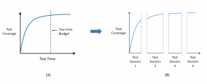
Logic BIST is another popular form of structural in-system test resource that can be accessed through the IST controller. This test solution involves the on-chip generation of random patterns that are applied to scan chains to test the logic portion of a chip. The circuit responses to all of the random patterns are accumulated into a signature, which is examined at the end of the test for a pass/fail result. The test coverage achieved by applying an increasing number of random patterns grows logarithmically as shown in Figure 4.
Figure 4: Managing Logic BIST test time
A common challenge in using this approach is achieving a high enough test coverage within a given time budget. A solution to this problem is to time slice the test into multiple sessions as shown in Figure 4b. Each successive slice is applied during an available break in the functional operation. For example, in an image processor used to process visual data, each test session could be applied in between processing individual image frames. Management of the multiple test slices requires careful coordination between the IST controller and logic BIST engine. The IST controller must keep track of which test slice is to be applied next, initialize the logic BIST engine to have it generate the correct set of random patterns, and then retrieve and compare the intermediate signature to determine pass or fail status.
In cases where this form of distribution either is not possible or still cannot provide the required coverage in the FTTI (Fault Tolerant Time Interval). New technology is available which significantly reduces the test time of these logic BIST monitors which in turn significantly improves their overall response time.
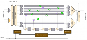
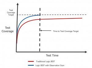
Logic BIST with Observation Scan Technology uses special test points inserted in the design along with a small dedicated scan chain of observation scan cells, which can effectively capture fault coverage of the functional logic, on every shift cycle, as opposed to only on the capture cycle of each pattern. As shown here in Figure 5.
Figure 5: Logic BIST with Observation Scan Architecture
The result in a lot faster ramp in coverage for the functional logic, enabling these safety mechanism’s to reach their required quality goals a lot quicker than using traditional logic BIST. Figure 6 shows how this ramp compares between LBIST-OST and traditional logic BIST.
Figure 6: Test Time Improvement with LBIST-OST
All of these technologies and methodologies described above enables any number of system level safety-related functions to be implemented. Key-on and key-off tests can easily be accomplished by sending out commands to all IST controllers to have all test resources run specific tests, depending on the scenario selected Any test failures can be reported back to the safety manager, which can use the results to drive some form of corrective action from something as simple as displaying a warning message on the dashboard to powering down the vehicle for further service.
The IST controllers can also be instructed to run periodic tests while the vehicle is operating on portions of the electronic system that are involved in safety-critical functions. Again failing results from these tests would can be monitored by the safety manager and the appropriate response can be taken, this could be as simple as disabling specific ADAS functions or as drastic as putting the vehicle into some safe operational state. This is where the response time of these safety mechanisms discussed above becomes critical.
The need for regular in-line monitoring of automotive electronic systems will no doubt continue to grow as the amount and complexity of safety-critical functions continue to expand. Some commercial solutions to address this need have already been introduced and no doubt will continue to evolve over time.
 Lee Harrison is Automotive IC Test Solutions Manager within Mentor’s Tessent group and has responsibility for the company’s automotive test solutions. His previous position was manager of DFT consulting services at Mentor, where he managed a worldwide team of consultants delivering DFT and test solutions in many different product domains. He has also held senior engineer positions at 3COM and BAE Systems. He received his Beng in Microelectronics and Brunel University, London, UK.
 Electronics Weekly Electronics Design & Components Tech News
