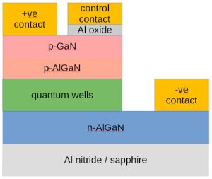
They took the idea of driving an LED via a hybrid-T network, which combine ac and dc drive signals, one stage further, building a capacitively-coupled ac control electrode onto a conventional GaN LED structure.
The control electrode alters the number of holes in the p-GaN – Al2O3 region (see diagram), which varied from around 1016/cm3 with +10V on the extra electrode, up to ~1020/cm3 with -10V.
The extra electrode does not affect the colour of the output – it remains a 270nm UV LED – but it does modulate the light output.
With a 2mA constant current applied through the p- and n-metal contacts of the diode, and a 10MHz sinewave on the third terminal, “approximately 25µW of output is produced at no bias, and a 20Vpp 10MHz signal results in approximately 31.4µW of output. Thus, the modulation depth is around 25% with a +/-10V signal,” researcher Muhammad Hunain Memon told Electronics Weekly.
In the proof-of-concept device, the positive contact and control contact are inter-digitated on the top surface of the device, whose active area measures 200 x 200μm.
To see how modulating the device via its third terminal compared with modulating a convention LED via an external hybrid-T network, the team build a similar sized conventional LED.
The three terminal version modulated up to ~263MHz, while the two-terminal version ran out of steam at ~160MHz.
Using 32, 16, 8, 4 and 2 QAM (quadrature amplitude modulation) the team managed to send up to 1.288Gbit/s across a short distance.
The device is also photo-sensitive, with the researchers demonstrating that the third terminal allows NAND and NOR logical operations on performed on optical digital signals as they are received and converted to electrical signals.
USTC worked with Fudan University, The Australian National University, King Abdullah University of Science and Technology, and Wuhan University.
The research has been published as ‘A three-terminal light emitting and detecting diode‘ in Nature Electronics – only the abstract can be read without payment.
 Electronics Weekly Electronics Design & Components Tech News


