“Many mosfet manufacturers focus on achieving high efficiency through low Qg(total) and low Qgd, when benchmarking the switching performance of their devices against alternative offerings,” said the company. “However, Nexperia has identified Qrr as being just as important due to its impact on spiking and, in turn, the amount of electromagnetic interference (EMI) generated during device switching.”
It has not handed out figures for these parameters, so, randomly selecting the 8 x 8mm, 80V, 2.3mΩ, 240A, n-channel PSMN2R3-80SSF, the data sheet figures are:
- Qg(total) 61 – 184nC (123nC typ) – 25Ad, 40Vd, 10Vg, 25°C
- Qgd: 7 – 51nC (22nC typ) – same
- Qr: 47nC typ (no max/min) – 25As, -100A/µs, 0Vg, 40Vd, 25°C
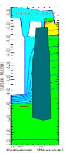
According to the company, to reduce on-resistance it has as decreased epi thickness and increased doping to increasing epi conductivity.
Partly to cope with increased doping, surface fields have been reduced (left) by deep trenches with oxide enhancement and an embedded source field plate.
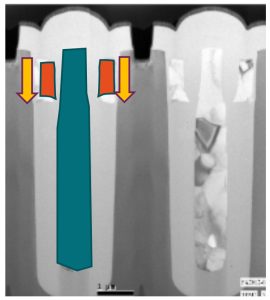 Right:
Red: smaller gate structure
Blue: deeper surface implant
Yellow: shorter conduction channel
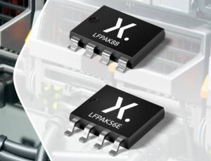
The choice of legged packaging is deliberate – the added flexibility reduces the chance of mechanical failure due to thermal cycling.
Further devices are planned in 12 x 12mm CCPAK1212 packaging, which also has flexible legs, and also in the pipeline is a 1.2mΩ 80V 8 x 8mm LFPAK device.
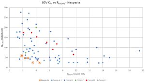
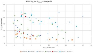
Get an idea of the range of 80V (left) and 100V (below) devices from these graphs – as the generations and companies are not mentioned, take the ‘competitor’ figures with a pinch of salt.
Nexperia’s mosfets are manufactured on a new 200mm line in Manchester UK.
Find the 1.2mΩ 80V 8 x 8mm PSMN2R3-80SSF product page here
 Electronics Weekly Electronics Design & Components Tech News
