ST has named it MasterGaN1, and is aiming it at consumer chargers and power adaptors, and industrial applications up to 400W.
GaN transistors are fast and efficient, allowing considerable size shrinks in ac-dc power supplies compared with those using silicon mosfets. However, GaN transistors (which are all HEMTs) are fussier to drive than silicon mosfets, creating a considerable barrier to adoption.
“Today’s GaN market is typically served by discrete power transistors and driver ICs that require designers to learn how to make them work together for best performance. MasterGaN bypasses that challenge,” said ST.
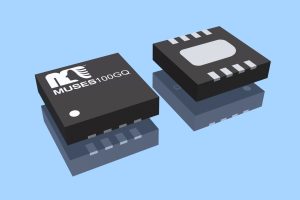
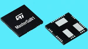 MasterGaN1 comes in a 9 x 9 x 1mm GQFN package with over 2mm creepage distance between high-voltage and low-voltage pads.
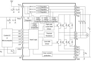
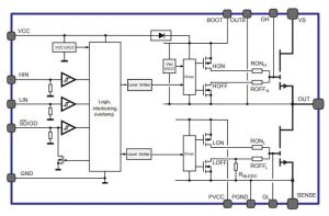
The two GaN transistors are normally-off and rated at 10A and have 150mΩ Rds(on).
The device’s logic inputs are compatible with signals from 3.3V to 15V, and built-in protection includes over-temperature, and low-side and high-side under-voltage lock-out. UVLO protection.
Inputs are:
- low-side driver inputs (hi=on, internal pull-down)
- high-side driver inputs (hi=on, internal pull-down)
- shut-down
An interlock stops both output transistors coming on together.
Operation is over -40°C to 125°C.
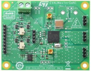 An evaluation board is available
A family of MasterGaN devices are planned, for use in topologies including: fly-back, forward with active clamp (see data sheet for example), resonant and ‘bridgeless’ totem pole PFC, as well as “other soft- and hard-switching topologies used in ac-dc and dc-dc converters and dc-ac inverters”, said ST.
 Electronics Weekly Electronics Design & Components Tech News
