Key to the development is the identification, by University of Southampton researchers, that a PCB manufacturing plant has everything needed to make micro-fluidic bio-chemical sensors. Disposable cartridges made like PCBs would clip into a hand-held analyser – also being development at Southampton.
The idea is to automate the ‘enzyme-linked immunosorbent assay’ (ELISA) process – the gold standard for detecting certain viruses and protein expressions, according to Southampton scientist Dr Themis Prodromakis.
Currently, said Prodromakis, ELISA is either fully manual – involving someone dripping liquids into small containers with a pipette – sometimes periodically for up to 12 hours – or it is done automatically by something akin to inkjet printing – which is expensive enough to require one machine in a central office to serve multiple medical facilities.
Microfluidics machined into silicon on a CMOS-like process is another alternative, which offers extreme parallelism – good for DNA analysis – and very cheap chips – in the order of 1p he said. Unfortunately this 1p can increase up to $200 when the associated fluid interfaces have been added to the chip. If only a few simple tests are needed, say under 100 virus checks, this is expensive over-kill.
Prodromakis believes that all the appropriate fluidic channels, coated electrodes, and other features necessary for ELISA can be made on a normal PCB production line using standard routing and plating. If the sub-mm channels achieved with normal routing are insufficient, micro-scale channels can be formed with the laser routing now becoming available in PCB plants.
The pumps, valves, and reagent chambers (plus display, controls, and sensor electrode amplifiers), will be in the non-disposable hand-held into which the sensor cartridge snaps.
Samples would be injected into either the disposable or permanent part – there are different strategies – and a button pushed to set the device going.
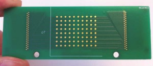 “It doesn’t need to be super-engineer. The cleverness is in the design of the disposable cartridge. It just needs simple PCB electrodes and microfluidics,” said Prodromakis. “We already have preliminary data. We have demonstrated the concepts in research over the last few years.”
Analysis times will stay the same – it will still take 12 hours to run a protein expression test, but the tests will be fully-automatic, and done on the spot.
“It will be portable, and valuable because of the lower cost. You could use it in Africa. It will be extremely versatile – HIV or TB tests will need a couple of disposables and a few minutes,” said Prodromakis.
How about injection-moulding the disposable part?
This option is attracting much interest because injection moulding it is so cheap, according to Prodromakis, however the basic cost increases dramatically once the electrodes and multiple materials needed for ELISA are added.
Because of the multiple materials involved – which cannot be discussed because of the patent situation – he sees a PCB-like manufacture as the better alternative.
The EPSRC has allocated £1m for the three year project. This mostly goes to Southampton, although some of it will pay for a clinical research fellow at Imperial College NHS Trust to bench-mark the equipment as it develops against conventional ELISA.
PCB maker Newbury Electronics is providing manufacturability consultation for free, and has offered to make the prototypes.
“A project of this nature is the perfect illustration of how academia, manufacturing and the end-user can pool their knowledge and experience. There is a real opportunity for this new diagnostic tool to make a tangible difference to healthcare,” said Prodromakis.
Newbury specialises in small quantities of PCBs. “We do 15,000 different types of circuit board every year, and work with Imperial and Southampton a lot,” Newbury MD Philip King told Electronics Weekly.
According to King, channels 0.5mm wide can be routed into the layers of a multilayer PCB for fluid channels, and sensors can be made using normal metal tracks.
The first stage is underway, with researchers from Southampton and the manufacturing team from Newbury thrashing out how theory and practice can be combined, and deciding which alternative materials suit both theory and practice.
“We will inevitably learn new methods and techniques. Working at the leading-edge puts us in a great position to maximise on any commercial opportunities that might arise,” added King.
 Electronics Weekly Electronics Design & Components Tech News

