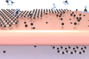
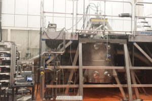
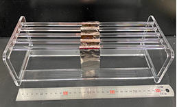
As the first phase of the Graphene Flagship’s 2D Experimental Pilot Line (2D-EPL) project draws to a close, some of the partners provided an update on its progress to establish a European ecosystem and move graphene wafers out of the laboratory environment and into full wafer production. One of the partners, Graphenea, manufactures and commercialises different graphene materials. Its scientific ...
Tag Archives: graphene
Black Semiconductor raises €254m for graphene ICs
Black Semiconductor, the four year-old German startup pursuing graphene ICs, has secured €228.7 million from the German Ministry of Economic Affairs and Climate Action and the state of North Rhine-Westphalia over the next 7 years under the EU support structure IPCEI ME/CT. Alongside the public funding, Black Semiconductor has raised €25.7 million in equity funding. The round was led by ...
Sensing lactic acid with a graphene-like foam capacitor
University of Bath researchers have created a lactic acid sensor using double-layer capacitance created when a particular sensitive molecule is attached to a graphene-like porous electrode structure and immersed in a buffer solution. Creating an ac-based capacitive sensor, as opposed to dc voltage or current based sensor, sides-steps concentration and chemical consumption issues encountered in battery-like reactions. The carbon material, ...
Graphene Flagship symposium highlights 2D-EPL foundry production
A symposium hosted by the Graphene Flagship (11-12 June) at the Town Hall Europe, Brussels will review the €20 million 2D Experimental Pilot Line (2D-EPL) graphene foundry project. It foundry integrates graphene and other 2D materials into semiconductor devices. The 2D-EPL project is a four-year project, started in October 2020, intending to produce graphene and related materials in a scalable, ...
Novel graphene-like foam sensors detect lactate for medicine
Graphene-like foam sensors from Stirlingshire-based Integrated Graphene can detect lactate concentrations for medical and fitness applications, according to research at the University of Bath. The company describes its patented substrate as “a three-dimensional carbon-based nano-material consisting of twisted multi-layers of atoms arranged in a honeycomb structure”. To form a lactate-detecting electrode, boronic acid was absorbed into the foam, and then ...
Bio-electrodes are injectable temporary gels
Researchers at the Gwangju Institute of Science and Technology in Korea have developed injectable bio-electrodes with pre-settable lifetimes. “In recent times, conductible hydrogels have attracted great attention as bioelectrode materials owing to their flexibility, compatibility, and excellent interaction ability,” according to the Institute. “However, the absence of injectability and degradability in conventional conductive hydrogels limits their convenience of use and performance ...
What caught your eye this week? (ChatGPT, Graphene FETs, Mining IoT)
The Electronics Weekly team share some fingerposts - their picks of the week, in terms of announcements, developments, product releases, quotes or anything else in the wide world of electronics that caught their eye…
Single crystal graphene grown on sapphire
Researchers in Saudi Arabia have grown wafer-scale single crystal graphene on insulating substrates. “If graphene can be grown on an insulating substrate with a clean interface, certain devices might function better,” said project scientist Bo Tian of KAUST – the King Abdullah University of Science and Technology. “This also opens the door to new types of graphene-based nanodevices.” The technique ...
Paragraf launches graphene sensors
Paragraf, the Cambridge graphene component specialist, has announced the availability of a new sensor range capable, it claims, of unmatched sensitivity and linearity when placed in low temperature environments and in strong magnetic fields. Tested at the High Field Magnetic Laboratory (HFML) at Radboud University Nijmegen, the GHS-C sensors support operation in magnetic fields up to 30 T and at ...
Almost perfect graphene grown
Korea’s Institute for Basic Science (IBS) has grown what is thought to be the most perfect artificial graphene yet – with no wrinkles, folds or ‘adlayers’ (islands of multiple-layer graphene) – using a process that appears to be scalable to larger quantities. The same team, from IBS’s Center for Multidimensional Carbon Materials (CMCM), had previously reported single-crystal adlayer-free films of graphene, but ...
 Electronics Weekly Electronics Design & Components Tech News

