“These new LinkSwitch-TN2 ICs are pin-to-pin compatible with previous generations, making it simple for customers to upgrade to higher-power designs,” according to the company. “A buck converter can be created using a minimal number of components.”
Called LNK3207, the chip can create a converter with >80% efficiency and <30mW no-load consumption. Inside is a 725V power mosfet, a jittered oscillator, a high-voltage switched current source for self-biasing, cycle-by-cycle current limiting, hysteretic thermal shutdown, output over-voltage protection and input over-voltage protection.
The controllers regulate by on-off control, skipping cycles in response to a signal applied to the feedback pin – greater than 49μA into the pin inhibits switching of the mosfet. The result is only a few cycles are skipped at full power wile many are skipped at low load reducing effective switching frequency.
There are three parts:
- LNK3207P – PDIP-8C package
- LNK3207G – SMD-8C package
- LNK3207D – SO-8C package
“The SMD-8C package is ideal for high-temperature ambient 85/105°C applications,” said the company.
Mass-market appliances applications are envisaged, such as washers, dryers and coffee makers, as well as in low-power sensor-based devices such as home security cameras, smart thermostats, metering and IoT installations.
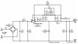
 A reference design (RDR-912 right) describes a 6.6W non-isolated buck converter built around the chip with the aim of producing 12V 550mA from 85 – 265Vac with the lowest possible component count. Its characteristics include:
- 725 V maximum drain voltage
- No optocoupler required for regulation
- Thermal overload protection with automatic recovery
- >80% efficiency at full load
- <±5% load regulation
The LNK3207 is included on this LinkSwitch-TN2 page
Reference design RDR-912 can be found here
 Electronics Weekly Electronics Design & Components Tech News


