Electronics Weekly has delved inside to see how it works.
In essence, the CNT logic is CMOS, as the researchers have found a way to create p-channel CNT mosfets and n-channel mosfets with balanced characteristics, these transistors do use metal oxide insulators, and they have been built into boolean logic gates using the same circuits used in silicon CMOS.
How they have managed to do this is summed up into three acronyms coined by the MIT team, described below: RINSE, MIXED and DREAM.
Which processor
Before all that, a few words about the processor.
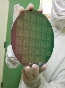
Dubbed ‘WRV16X-Nano’, it occupies 7 x 7mm on a die (32 die/wafer), runs from 1.8V, and executes one of the RISC-V instruction sets: the 32 instruction RV32E. Instructions are 32bit, the data path is truncated from 32bit wide to 16bit, the address bus is 16bit , and its register count is reduced from 16 to 4.
This is assembled form 14,702 CNT mosfets in 3,762 logic stages, with paths up to 86 cascaded logic stages between flop-flops – which means they must settle within one clock cycle – on the subject of clocks, the main clock is external, but all control signals from that are generated with CNT logic.
Main memory is off-chip dram.
Transistor architecture
The transistor channels sit in the middle layer of a five-layer stack that takes over a hundred processing steps to complete:
- Metal layer 5: power distribution
- Metal layer 4: n-mosfet source and drains
- Metal layer 3: p-mosfet source and drains, and inter-cell routing
- Carbon nano-tubes: laid horizontally
- Metal layer 2: gates and signal routing
- Metal layer 1: signal routing
- Substrate
The transistors are bottom-gate, and the metal-under-transistor structure is possible because CNT deposition and post-deposition processing is low-temperature – and is actually solution-based.
There is a thin oxide gate insulator between Metal layer 2 and the nano-tubes.
 Problems with carbon nanotubes
In the MIT process, the CNTs are bought from a commercial source, rather than grown in-situ, and solution-processed into an even flat layer using only air-stable chemicals.
The first major issue that, and well as lying down obediently on the substrate, nano-tube are prone to forming tangles bundles or balls when they are solution-processed.
Any bundle left on the surface when the next metal layer is deposited is a potential failed transistor.
Sonication – like ultra-sound cleaning – is one way to remove the bundles, but applied conventionally it also tears off patches of wanted planar CNTs
RINSE
RINSE – removal of incubated nanotubes through selective exfoliation – is MIT’s answer to keeping planar nanotubes while removing tangle balls.
Key to RINSE is applying a thin coating of adhesive (actually a re-purposed photo-resist) to the raw CNT layer that solidly sticks the bottom layer of planar CNTs to the substrate, but cannot effectively bond the tangles to the substrate.
This alters the balance of adhesion, allowing sonication to break the tangles free without removing the bottom layer of planar CNTs – even hours of sonications can not shift the planar layer.
The result is >250x reduction in tangle balls, with no effect on the planar layer that can later be measured in mosfet performance.
MIXED
Left to their own devices, the n and p-channel CNT mosfets would not have equal transfer characteristics – resulting logic would not have input characteristics symmetrical about Vcc/2 (900mV in this case), which is where MIT’s MIXED – metal interface engineering crossed with electrostatic doping – comes in.
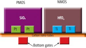 The key parts (see diagram) are:
- Electrostatic doping – choosing an appropriate metal oxide passivation layer over the source, drain and channel of each transistor, then depositing it (using atomic-layer deposition) with a selected non-stoichiometric amount of oxygen – giving it a permanent electric field that will bias the transistor’s CNT channel, and changing the behaviour of the oxide-CNT interface.
- Work-function engineering at the source-CNT and drain-CNT contacts.
The p-mosfets get platinum (high work-function) contacts and SiOx (where x is adjusted from 2) passivation
The n-mosfets get titanium (low work-function) contacts and HfOx (would be HfO2) passivation
As well as controlled threshold voltages, this technique improves the the on/off state current ratio in both n and p devices, while only using material found in silicon CMOS.
DREAM
One of the characteristics of CNTs is that, due to variation in diameter and chirility, in any batch some are semiconducting and some conduct metallically – the latter acting as an unwanted fixed resistor across any mosfet they get built into.
Pre-processing can reduce the number of metallic CNTs in a batch, with more pre-processing reducing the numbers of rogue CNTs (at a price) but, practically, they cannot be eliminated.
DREAM – designing resiliency against metallic CNTs – is the team’s way of dealing with the inevitable presence of metallic CNTs.
It does not need chemistry, or process engineering, and instead relies on circuit design.
The metallic CNTs are hardly ever hard short-circuits if they get into a transistor channel, but are instead permanently resistive to some extent.
This gives any transistor they get into a ‘soggy’ characteristic, and reduces the static noise margin of any Boolean gate the transistor ends up in.
To get some statistics, 1,000 p-mosfets and 1,000 n-mosfets were made, scattered across a wafer, and their Vds, Id and Vg characteristics measured – as an aside these transistors have ~15-25 CNTs per channel.
The data from these 2,000 transistors was used to simulate the input/output voltage characteristics of one million two-input logic gates.
Then pairs of these simulated gates were modelled, one driving the other.
It was discovered that, considering the schematics (and physical layouts – the nanotubes are long, introducing some correlation) some pairs statistically had a far better static noise margin in the presence of occasional metallic CNTs that others.
NANDs driving NANDs, and NORs driving NORs, are far more tolerant than NANDs driving NORs, or NORs driving NANDs.
These observations were used to create a custom ‘process design kit’ and a custom 63 entry ‘standard cell library’ for the EDA tool-chain – a mix of standard Synopsys, Cadence and Mentor Graphics semiconductor tools.
Using only metallic-CNT-tolerant gate combinations, according to MIT, reduces the CNT raw material purity requirement from 99.999999% (one metallic amongst 100 million semiconducting CNTs) to 99.99% (one metallic amongst 10 thousand semiconducting CNTs ) – a 10,000x improvement – without imposing any extra processing steps or needing redundant logic blocks.
99.99% is already commercially available and can be achieved through several means – including solution-based sorting, which was used to prepare CNTs for RV16X-Nano, according to the team, adding that the average transistor had a gain of >15 and that the optput voltage swing of logic was typically 99% of Vcc, but down to 70% in metallic CNT-affected outliers.
 Much of the information above comes from the well-written Nature paper: ‘Modern microprocessor built from complementary carbon nanotube transistors‘ which describes the work in great detail.
However, it provides only static transistor and logic characteristics and does not include any timing or speed information. Information provided alongside the paper shows the CPU is predicted to run at over 1MHz, but due to test gear limitations is was only run at 10kHz during the research – where power consumption was just under 1mW, and dominated by leakage.
~1MHz peak operation was “due to the relaxed technology node, as well as us not optimising for performance”,Max Shulaker, corresponding author on the above paper, told Electronics Weekly. “The goal of this work was demonstrating functionality. Our next goal, now that we know we can build chips that work, is to build chips that give performance benefits.”
In 2013, while at Stanford University, Shulaker published ‘Carbon nanotube computer‘, a paper describing the build of a one-bit CPU using 178 carbon nanotube mosfets that implemented 20 instructions from the MIPS instruction set.
 Electronics Weekly Electronics Design & Components Tech News

