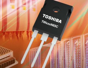
 Toshiba is claiming better improved on-resistance and gate charge for its third generation of industrial 650V enhancement-mode silicon carbide mosfets.
The “third generation SiC process optimises the cell structures used in second-generation devices,” according to the company. “As a result, the product of Rds(on) and Qg, that represents both static and dynamic losses, has improved by about 80%”.
In common with earlier devices, to enhance reliability, the mosfets include a SiC Schottky barrier with -1.35V (typ) forward voltage to suppress fluctuation in Rds(on).
There are five devices, all in TO-247 packages: TW015N65C, TW027N65C, TW048N65C, TW083N65C and TW107N65C
Picking the flagship TW015N65C: it handls 100A abs max and its on-resistance is typically 15mΩ (21mΩ max, Vg = 18V Id=50A) and gate charge 4.85nF typically (Vds=400V Vg=0V 100kHz). Rise and fall times are 79 and 59ns, turn-on and turn-off times are 117 and 116ns (fig 6.2.1 in data sheet for caveats).
Gate threshold is kept high at 3.0-5.0V (Vd=10V Id=11.7mA) to make the mosfet “less susceptible to malfunction”, said Toshiba
Applications are foreseen in switch-mode power supplies and uninterruptible power supplies for servers, data centres and communication equipment, as well as in photovoltaic inverters and in bi-directional electric vehicle chargers chargers.
The TW015N65C product page is here from which the data sheet can be downloaded.
—
 Electronics Weekly Electronics Design & Components Tech News
