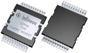
Dubbed QDPAK and DDPAK (in-use, below left), they are intended to replace through hole TO247 and TO220 (respectively) and “deliver equivalent thermal capabilities with improved electrical performance”, said Infineon. “JEDEC package registration, according to MO-354, serves as an enabler for the transition of high-voltage industrial and automotive applications to top-side cooled designs.”
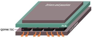 The footprints are 15 x 21mm and 6.5 x 21mm respectively, and the company standardised package height at 2.3mm for planar heatsink contact, although “in reality, not all packages will have the same distance from package top to cold plate due to manufacturing decisions. Therefore, the height tolerances must be balanced with some kind of thermal interface material”, it said.
There are two 15mm packages, with different thermal pad sizes. All of the packages have cut-aways which allow visual inspection of the pad-to-PCB solder joint.
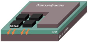
Infineon’s idea of heatsinking before top-side cooling
The company also emphasises that the top-side cooling allows drivers to be places close to the power switches, decreasing drive loop size and therefore drive loop inductance which reduces ringing on gate lines.
I subtlety of the packages is that underside is up to 150μm off the PCB when the legs land on its surface. “One benefit of the stand-off is that a standard stencil height for reflow soldering can be used,” said Infineon. “With a positive stand-off, no extra board cleaning is required before the SMD device is placed on the PCB for reflow soldering. This enables direct contact between the pins and the solder stencils.”
Infineon has an excellent techncial backgrounder on these packages
 Electronics Weekly Electronics Design & Components Tech News
