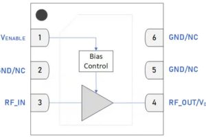
Component distributor Richardson RFPD is stocking a 5 to 8GHz GaAs pHEMT low noise linear amplifier from Guerrilla RF, and has added it to its design support service. Measuring 1.5 x 1.5mm (DFN-6), GRF2110 is aimed at WiFi 6/6E, small cell and wireless infrastructure. It operates from 2.7 to 6V, drawing 70mA at 5V. Power is applied to the output ...
Tag Archives: GaAs
Laser vision will develop new markets
Epitaxial regrowth and GaAs can unlock new semiconductor laser markets, argues Richard Hogg. Design engineers might use epitaxial regrowth to enhance semiconductor laser performance and unlock new markets. Relatively mature epitaxial regrowth process for indium phosphide (InP) lasers are commonly used in 5G, datacom, telecom and co-located optics applications. Gallium arsenide (GaAs) is a less mature material system, which suits ...
It’s GaAs GaAs GaAs
RF front end component manufacturers are turning to GaAs as their main material of choice
Inter-metallic bonding stacks GaAs and Si solar cells
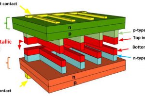
Inter-metallic bonding could remove unwanted carrier barriers from multi-junction solar cells assembled by stacking finished single-junction cells, according to North Carolina State University. “We want to create high efficiency solar cells at a reasonable cost,” said engineering professor Salah Bedair. “Silicon-based thin solar cells are very popular because the material has around 20% efficiency and the cells cost about 1/10th what ...
GaAs up/down converters offer side-band choice
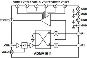
ADMV10x RF up/down converters are GaAs MMICs from Analog Devices, aimed at a variety of audio and video data transmission applications: satellite communications, radar, electronic warfare systems, and point-to-point radios are singled out by distributor Mouser, which is stocking all the ADMV10x parts. ADMV1009 is a single side-band (SSB) I/Q up-converter optimised for point-to-point microwave radio designs operating in the 12.7 ...
UK foundry adds RF GaN
Newcastle-based Inex Microtechnology is to use Keysight’s Advanced Design System (ADS) EDA software to deliver its gallium nitride (GaN) Process Design Kit (PDK) “Our GaN HEMT process addresses a growing UK space and defence customer base. The process developed over the last two years enables a unique UK sovereign supply,” said Inex CTO Matthew O’Keefe. “We aim to provide our ...
Glasgow University works with local firms on single photon detectors
CST Global, the Glasgow-based III-V opto-electronic, semiconductor foundry, is collaborating with the University of Glasgow and Gas Sensing Solutions on a project to fabricate active matrix, single-photon GaAs devices. The project will develop light-weight, monolithic, mid-wave infrared (MWIR) imagers, capable of detecting a single photon of IR light. These are primarily used to image gasses and diagnose their composition. Dr ...
Simple surface nano-particles could improve LEDs
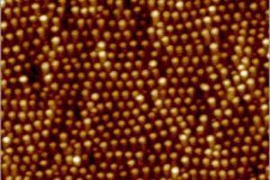
Predictable arrays of plasmonic nano-particles can be grown on the surface of LEDs to improve photon emission by localised surface plasmon resonances, according to the University of Michigan. “The idea of adding nano-particles to increase LED efficiency is not new, but previous efforts to incorporate them have been impractical for large-scale manufacturing,” said the University. “They focused on pricey metals ...
1µm GaAs laser made on silicon
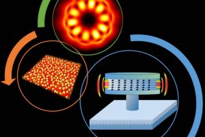
Scientists have fabricated GaAs lasers directly on silicon. Nano-scale patterns were designed and created on the silicon to confine lattice mismatch defects which “made the GaAs-on-silicon template nearly defect free, and quantum confinement of electrons within quantum dots grown on this template made lasing possible”, said Applied Physics Letters, where the work has been published. The lasers work in ‘whispering ...
Laser wires grown on silicon
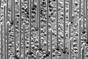
Physicists at the Technical University of Munich (TUM) have grown GaAs laser wires on silicon. Lattice mis-match makes growing GaAs on silicon difficult, which is why Dr Gregor Koblmüller and Professor Jonathan Finley are building the lasers vertically. “The two materials have different lattice parameters and different coefficients of thermal expansion. This leads to strain. Planar growth of GaAs onto ...
 Electronics Weekly Electronics Design & Components Tech News
