Kishida said that the importance of the fab is that Japan “is now being positioned as an important foothold in TSMC’s world strategy.”
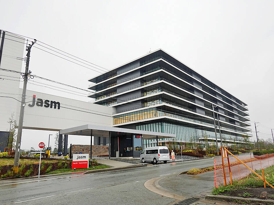
The fabs are owned by a jv called JASM (Japan Advanced Semiconductor Manufacturing) in which TSMC, Sony, Denso and Toyota hold equity stakes of approximately 86.5%, 6.0%, 5.5%, and 2.0%,
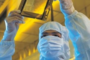
Kumamoto 1 (pictured) which cost $8.6 billion and had a $3.2 billion subsidy from the government, will have total capacity of 40–50k wpm focusing mainly on 22/28nm processes with some 12/16nm starting in Q4, and Kumamoto 2 will run a 6nm process starting in 2027. The total capacity of both fabs combined will be 100k wpm.
At the opening ceremony Morris Chang, the founding CEO of TSMC, said that the fab “will, I believe, improve the resiliency of chip supply for Japan and for the world. It will also, I believe, start a renaissance of semiconductor manufacturing in Japan.”
After Kumamoto 2 , TSMC is planning a third fab in Japan for which it is currently looking for a location. The third fab will initially be focussed on 6/7nm processes leading to 5nm or 3nm processes.
TSMC’s establishment of a 3DIC research center in Ibaraki and plans for an advanced packaging plant in Japan will give it a comprehensive chip manufacturing presence in Japan.
Japan is developing three semiconductor manufacturing hubs in Kyushu, Tohoku, and Hokkaido where Rapidus is targeting the 2nm process.
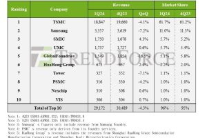
2023 global foundry revenues hit $117.47 billion, with TSMC taking a 60% share, says TrendForce, and this is expected to rise to around $131.65 billion in 2024, increasing TSMC’s share to 62%
 Electronics Weekly Electronics Design & Components Tech News
