As such, production lead time is reduced – the target is two weeks by December 2020, according to company CEO David Summerland.
Using just those eight layers, he continued, it is also possible to include power and analogue components.
Key to the whole scheme, branded Bizen, is a novel transistor – essentially a pnp device whose base is driven through a quantum tunnelling junction, and which includes a second tunnelling junction to internally self-bias the transistor – more of the technology later. It is, said Summerland, starting out on silicon, but is capable of migrating to GaN and other compound semiconductors.
Silicon Bizen is not just a theoretical exercise: Search For The Next has teamed up with established Glenrothes-based chip make Semefab, which is already running Bitzen wafers.
Together, the two firms aim to make technology demonstrator sample chips available to potential customers in Q2 next year.
For creating VHDL there will be a free-to-use process design kit (PDK) for Cadence, and standard libraries, making Bizen “80-90% faster to manufacture than CMOS”, according to Summerland.
 Bizen transistor
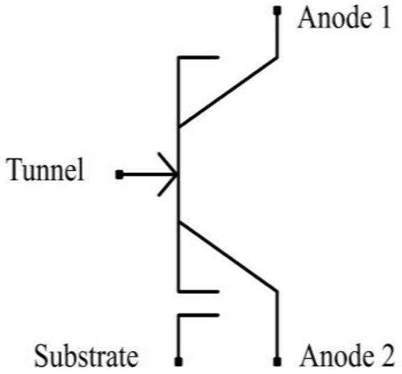
SFN’s transistor has a pnp-like structure, but with a difference at the base.
Update: According to Summerland in 2022, the transistor that the company is offering for logic use in 2022 is no longer the bipolar device described here. There is a 2022 update here
“It is a bipolar mechanism, not mono-polar like a mosfet,” said Summerland. “You don’t have direct contact to the base like a BJT, and it is not oxide-isolated like a mosfet. Instead there is a tunnelling junction to the base well with heavy doping and an abrupt junction. The result is Bizen – bipolar-zener – which retains the advantages of traditional bipolar processing yet removes the disadvantages by using Zener quantum tunnel mechanics.”
While the names ‘collector’ and ’emitter’ could have been used for the two non-tunnel (‘base’) electrodes, the device is symmetrical – those two terminals can be swapped without a functional change, according to SNF, so it has chosen to name them ‘anode 1’ and ‘anode 2’.
A second tunnelling junction, represented by two horizontal lines in the device diagram, biases the device so that it is ‘on’ (but not saturated) when the tunnel terminal is open-circuit. While this represents a continuous current flow to ground during operation, tunnel current is typically only 2-5nA, according to Summerland, who added that a lower-power ‘sleep’ mode can be introduced by including a single structure that can disconnect the bias tunnelling junctions of many – perhaps a thousand – bizen transistors from the negative rail.
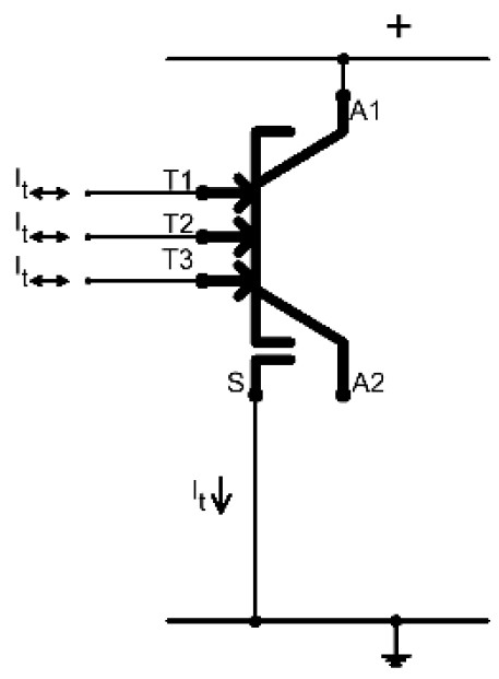
 Bizen three-input NOR gate – this is current rather than voltage logic. Connect any input to the positive rail to stop conduction between anodes.
In this open-circuit condition, the tunnel electrode will float at 200-300mV below the most positive anode (see diagram left), and the device can pass 20-30nA between its anodes with a drop as low as a few millivolts across those anodes.
This enables one Bizen transistor to pull up ~10 tunnelling junctions of following Bizen transistors up to within millivolts of the positive rail -to use TTL parlance, it has a fan-out of ~10.
When the tunnelling connection of a device is pulled to the positive rail, the current path between its two anodes is turned off and the tunnel terminals of following devices are not driven – they are left to float.
As such, any logic built with Bizen transistors is current-based logic rather than voltage-based, and does not require space-wasting resistors or additional current sinks beyond the biasing tunnel junction.
According to Summerland, any arbitrary logic function can be implemented using Bizen transistors, and only four process lithography masks (instead of eight for the full process) are required to implement logic-only chips as transistor-to-transistor connections can be made within the four layers – no metal layers are required. As mentioned above, design tools are being prepared. “If we did an ARM or an x86 [processor], we would use a couple of metal layers for routing,” said Summerland.
 To the right (yellow) is a Bizen D-type master-slave flip-flop, requiring only eight transistors and occupying 45 x 37μm in this 1μm process example. No metal layers are required. On the same size process, the CMOS version (left, green) according to Summerland, would need 28-35 transistors and occupy 112 x 37μm (with 2.5μm metal contact, 89 x 30μm with reduced (1.3μm) metal contact window. 1μm is a relatively coarse process: “We have theoretically shown that we can scale the Bizen process and are currently investigating proving that,” he added.
What about power consumption – those quiescent nA will add up.
Yes, agrees Summerland, but dynamic power is far less with Bizen because it does not have all the power-wasting mosfet gate capacitance associated with cmos.
Power transistors
The eight layer process can also accommodate npn power transistors – up to 650V – and base drivers for those transistors, according to SFN.
Bizen actually grew from a need to spice-up bipolar chips according to Semefab CEO Allen James:
Semefab engaged with SFN, exploring ways to reduce smart power IC process complexity whilst retaining an ability to program the chip. Early suggestions were rejected because they could not meet the low mask count target required. Eventually, SFN hit on the idea of using the quantum tunnel effect of miniature, reverse-biased Zener diode structures. It transpired that the integration of conventional lateral and vertical bipolar structures can, with careful modelling, be designed to incorporate Bizen without undue additional process complexity. I was initially quite sceptical but having lived with the concept and seen early-stage results, it does indeed tick many of the boxes needed to disrupt the industry. It’s not so much a question that CMOS is flawed – although CMOS is prone to latch up and ESD. CMOS is low power, has passed the test of time and is generally reliable. However, it is complex and when integrated with power even more so. Complexity means longer lead times and higher cost.
But aren’t bipolar power transistors lossy?
No. argues Summerland, no more than power mosfets, and they don’t have to be slower either. “Mosfet transconductance is based on the square root of the drain current. BJT transconductance is proportional to collector current,” he said, “and transconductance is related to speed, unless the mosfet is much wider than long.” What ever the transistor type “it is more down to the driver stage. We believe a Bizen power IC will switch as fast as a mosfet of IGBT”.
The process design kit (PDK) includes 1A and 10A power transistors.
Analogue computing
The last trick up SFN’s sleeve is Bizen analogue blocks – op-amps and comparators (in the PDK), and even analogue computing blocks such as a divider – the analogue computing blocks avoiding using logic – and thus the associated ADC and DAC – in certain applications. Using a coarse-fine architecture, Summerland is predicting 1μW 1μs analogue division instead of ~20 instructions and ~100 instruction cycles if logic was employed. This analogue processing capability is being branded IPU for ‘instantaneous processing unit’.
Temperature range
SFN is predicting that chips using Bizen transistors and the associated process developed with Semefab will operate across -40 to +85°C, although for detailed figures more wafers need to be run. “We are at ‘technology readiness level’ 5,” said Summerland.
Tunnelling current is affected by temperature, but the firm will balancing process parameters and intended operating voltage (which spans 5V to 3V, and even lower is possible with different doping) to aim for the point where avalanche and Zener characteristics cross-over to minimise temperature coefficient.
Semefab’s James told Electronics Weekly: “Temperature coefficient will be a million miles away from the dark current leakags of a diode, which doubles for every 7°C.” Which prompted Summerland to add: “It is orders of magnitude less, which is why we chose tunnelling current and not leakage current.”
On the subject of readiness, James said that his company is validating the PDK now and predicts Bizen logic for Q2 next year and “the integration of op-amps and comparators may converge on to the same time-scale. We have done the vertical power transistor, although we are not at 650V yet”.
He emphasised how quickly his firm will be able to turn a Bizen chip design into silicon. “The process is not rocket science: it uses standard diffusion and standard wafer fab blocks. There is nothing esoteric. At 1μm feature size we are not even having to consider wafer planarisation – the technology is happy with the contours. We could do runs in two to three weeks.”
“There is still a way to go before Bizen becomes a commercial reality and we are still learning,” added James, “however Semefab and SFN are working flat out.”
Technology demonstrator
In Q2 next year a technology demonstrator will be available for potential adopters of the process to try.
SFN is not saying much about it, except to say that is will incorporate Bizen logic, analogue IPU and power.
Summerland told Electronics Weekly that it is likely to have a 800 x 800μm die with a 300 x 300μm IPU in the middle surrounded by features including a vertical power npn.
It is likely to be in something similar to a TO-92 plastic case, and may even just have three connections, he said, firmly refusing to reveal its intended function.
 Electronics Weekly Electronics Design & Components Tech News


