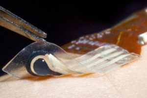
Health-related chemicals can be detected on dry skin, according to the National University of Singapore (NUS), which developed a stretchable ‘ionic-electronic bilayer hydrogel’ sensor with the Singapore Agency for Science, Technology and Research (A*Star). The chemicals are known as solid-state epidermal biomarkers. “These biomarkers, which include cholesterol and lactate, are found in the stratum corneum, the outermost layer of the ...
Tag Archives: Singapore
Si Box has $200m Series B; ramps chiplet production
Silicon Box, the chiplet packager founded by Marvell founders Sehat Sutardja and Weili Dai with Dr B.J Han, has raised a $200 billion Series B and is recruiting for 24/7 production at its $2 billion, 750,000 sq ft Singapore assembly plant. Founded in 2021, the company moved into volume production in Singapore last October. ”Silicon Box is well poised to ...
3d printing puts metal conductors anywhere on plastic parts
Researchers from Japan and Singapore have developed a 3D printing technique to create conductive metal patterns on the external and internal surfaces of 3D plastic structures. It does not print solid metal directly, but instead accurately positions a catalyst throughout a polymer object wherever surface metal will later be needed. Update: Harting is commercially offering a similar process using injection ...
UV modulation by twisting crystal films
Films of the two-dimensional material hexagonal boron nitride can be used to control light emission from materials, according to the Singapore-MIT Alliance for Research and Technology (Smart). The phenomenon involves the creation of ‘Moiré superlattices’ as two films are rotated with respect to one-another, and works at room temperature with films made from stacks of atoms around 100nm high – considered bulk materials ...
ST sets up lab-in-a-fab for piezo MEMS
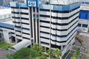
STMicroelectronics is setting up a 200mm piezoelectric MEMS research facility inside its existing semiconductor fab in Singapore, in conjunction with the Singapore research institute A*STAR’s IME and Japanese manufacturing-tool vendor ULVAC. The three companies have a history of working together. “This collaboration will accelerate the adoption of piezo MEMS actuators in new fields of application including MEMS mirrors for smart ...
Singapore is the most talented Asian nation
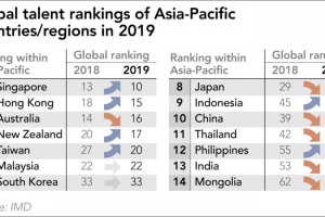
Singapore is top of the "IMD World Talent Ranking" of Asian countries mainly due to its high quality education.
Electronics Production Growth May Never Return, Except In China.
china accounts for over half of worldwide electronics production, say analysts Semiconductor Intelligence, and China should continue to be the key driver of electronics production growth for at least the next decade.
Good for China; bad for everyone else
China accounts for over half of worldwide electronics production, say analysts Semiconductor Intelligence, and China will continue to be the key driver of electronics production growth for at least the next decade.
Infineon and GloFo Developing 40nm Embedded Flash Process For 2015.
Infineon and GloFo are working on a 40nm embedded flash process for automotive and secure MCU applications for qualification in 2015.
Ten Most Indebted Countries
Thanks to economicshelp.org for this one – the ten most indebted nations measured by debt as a proportion of GDP:
 Electronics Weekly Electronics Design & Components Tech News
